What id the potential for high-frequency application of PCB-wound transformers?
PCB-wound transformer are a new type of transformer manufactured using printed circuit board(PCB)technology.By integrating the windings within the copper layer of the PCB,they replace traditional winding processes.Their development is closely tied to the electronics industry’s demand for higher frequencies,miniaturization,and integration.
A technology born for miniaturization
Traditional transformers typically have bobbins and utilize traditional winding methods,while PCB-wound transformers have neither bobbins nor windings.
In the early 21st century,continuous advancements in PCB manufacturing processes,such as the development of multilayer PCB technology and high-precision etching,provided strong support for the development of PCB-wound transformers.At the time,engineers,building on PCB technology’s approach to solving electronic device wiring problems,integrated the windings within the PCB and then attached a magnetic core to complete the transformer.
This technology was conceived specifically for transformer miniaturization.
At the same time,the performance of magnetic materials continued to improve,significantly enhancing the performance of PCB-wound transformers.During this period,PCB-wound transformers began to find application in a wider range of fields,such as communications equipment and computer power supplies.For example,Delta’s DC-DC modules used this type of PCB-wound transformer.
Advantages of PCB-wound transformers
PCB-wound transformer offer many advantage over traditional transformers.
Reduced production steps.PCB-wound transformers eliminate numerous steps,such as paint stripping,wire winding,casing,glue dispensing,and baking.This not only offers significant cost advantages but also a simpler structure.
Increased transformer power density.PCB-wound transformers can maintain a smaller size for the same power ,demonstrating strong competitiveness in terms of performance and cost.
Compared to traditional transformers, PCB-wound transformers can achieve over 50% higher power within the same volume.
Increased transformer efficiency.Traditional transformers achieve a ,maximum efficiency of only 92%,while PCB-wound transformers can achieve over 95%,and laminated flat-plate transformers can achieve over 98%.
Reduced transformer height. PCB-wound transformers excel in reducing transformer height. Hai Laibuqu, a national-level senior electrical engineering engineer and general manager of R&D at Huizhou Magnetic New Energy Technology Co., Ltd. (Magnetic New Energy), told Magnetic Components & Power, “Compared to conventional winding solutions, transformer height can be significantly reduced. We have a PCB transformer product that uses a PCB winding solution, reducing its height from 10mm to under 5mm.”
Strong consistency. PCB-wound transformers boast process tolerances within ±5%, far exceeding the ±20% tolerance of manual winding.
PCB-wound transformers have achieved multi-dimensional breakthroughs through process innovation, with core advantages reflected in manufacturing, performance, and structure. These technical attributes give them an irreplaceable competitive advantage in high-reliability fields such as industry and healthcare, providing key support for the miniaturization and high-frequency evolution of electronic equipment.
Application Scenarios of PCB-wound Transformers
These performance and size advantages have also led to the gradual rise of PCB-wound transformers.
New energy vehicles and charging infrastructure This type of product first appeared in the automotive sector. According to Wang Yao, “Automobiles, as major consumer goods, have high added value, allowing manufacturers to invest more in R&D to upgrade their products. Therefore, this type of product was first used in the automotive sector.”
New energy vehicles, due to space constraints, also require highly integrated magnetic components, and PCB-wound transformers can significantly reduce their size.
For example, current bidirectional on-board optical communication (OBC) systems typically draw power from both the high-voltage and low-voltage sides to power the entire controller circuitry. Therefore, the transformer has become a key factor limiting the height of the motor controller.
To address this pain point, Hangzhou Pujing Electronic Technology Co., Ltd. has designed a magnetically integrated PCB-wound transformer with a minimum height of 7 mm and is already working on designing even lower-profile transformer solutions.
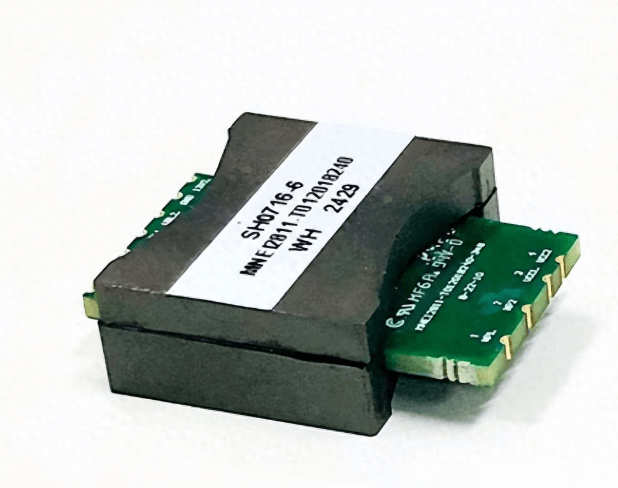
Magnetic integrated PCB winding transformer product

Magnetic integrated PCB winding transformer product, Image source: Pujing Electronics
Telecommunications power supplies. Later, Huawei and ZTE also began to gradually adopt this type of PCB winding transformer in their base station power supplies, leveraging the high-frequency characteristics and low-loss advantages of PCB winding transformers to optimize power module performance and meet high-frequency requirements.
Telecommunications power supplies must meet stringent requirements such as low voltage and high current, efficient voltage regulation, heat dissipation management, and high reliability. PCB winding transformers, through their multi-layer PCB layout, high-frequency magnetic core materials, and integrated design, can significantly reduce size, reduce conduction losses, and improve heat dissipation efficiency, making them an ideal choice for solving these problems.
For example, for high current requirements (e.g., above 20A), multiphase topologies are employed to reduce ripple current through phase interleaving. High current output can be achieved by connecting multiple controllers in parallel. PCB-wound transformers provide a compact magnetic integration solution for such designs.
Photovoltaic and energy storage inverters. High-frequency, high-power-density PCB winding designs are suitable for photovoltaic and energy storage inverters, optimizing energy conversion efficiency while meeting high-temperature and high-voltage requirements.
For example, the ultra-thin planar transformer developed by Shenzhen Yongchuangxing Technology Co., Ltd. combines two different processes: a primary printed PCB and a secondary copper foil plastic encapsulation. The resulting coil can pass higher currents, effectively addressing the manufacturing challenges of traditional wound transformers and meeting the low-voltage, high-current component requirements of photovoltaic inverters.
Consumer electronics and portable devices. Low-power products such as Huawei’s 65W GaN fast charger utilize PCB winding solutions to increase power density and reduce size, meeting the lightweight, thin, and compact requirements of portable devices.
Industrial automation and power equipment. Hailaibuqu previously mentioned the use of auxiliary transformers in rail transit, which must withstand 15,000V and require PCBs made of special insulating materials.
PCB-wound transformers are particularly well-established in busbar-type low-voltage power supplies, thanks to their compact size and simple structure.
Wang Yao also told Magnetic Components & Power Supplies, “PCB-wound transformers are most widely used in the industrial, medical, and military sectors, where reliability requirements are relatively high.”
PCB-wound transformers, with their performance and size advantages, began their application in the automotive sector. The high added value of the automotive industry drove product upgrades, leading to their initial application there. Since then, their application areas have continued to expand, including base station power supplies, industrial applications, and consumer electronics. Their advantages are particularly prominent in busbar-type low-voltage power supplies, and they are also finding application in low-power products.
Hailaibuqu also mentioned that this product structure is primarily used for auxiliary transformers and low-current inductors, and is used in low-power products such as formation power supplies and mobile phone chargers.
Currently, the main markets for PCB-wound transformers can be divided into five major categories: consumer electronics, new energy vehicles, renewable energy, industrial automation, and communications power supplies.
Some public data shows that the PCB transformer market size was US$3.1 billion in 2022 and is expected to reach US$5.7 billion by 2030. Benefiting from the continued demand for electric vehicles, renewable energy, and consumer electronics, it is expected to grow at a compound annual growth rate of 8.1% from 2025 to 2030.
Challenges of PCB-wound Transformers
However, PCB-wound transformers also have their limitations.
Generally speaking, the copper foil thickness of PCB boards must be between 2-5 oz (ounces), which limits the power ceiling and heat dissipation capacity of PCB-wound transformers. The power ceiling for a single PCB-wound transformer, or a single-layer board, is approximately 200W. Applications above 100W require integrated heat dissipation vias or a metal substrate.
This, however, increases the production cost of the PCB winding. While FR4 epoxy boards are commonly used in general industrial and medical applications, some high-end precision industrial equipment and aerospace applications may use aluminum substrates, which at least doubles the cost.
Combined with their simple structure, PCB-wound transformers are also unsuitable for applications with complex magnetic circuits.
Enargy, an industry engineer, told Magnetics & Power that this type of product was mass-produced for 3000W power supplies 20 years ago. However, subsequent iterations were gradually abandoned because they failed to achieve the desired reduction in size and cost, and were incapable of adapting to complex magnetic circuits.
This is also due to the power and heat dissipation limitations of PCB-wound transformers. As power levels increase, heat dissipation issues make PCB windings unsuitable.
To overcome the power limitations of PCB-wound transformers, an upgraded version of PCB technology was developed around 2005. This approach employed a laminated structure, stacking copper sheets layer by layer, what we now call a planar transformer, achieving even higher power output.
In the past two years, as magnetic integration technology has gradually penetrated high-power module power supply applications, PCB-wound transformers have once again attracted the attention of engineers.
We have noticed that a new type of magnetically integrated PCB-wound transformer with a PCB board + winding/coil structure has appeared on the market.
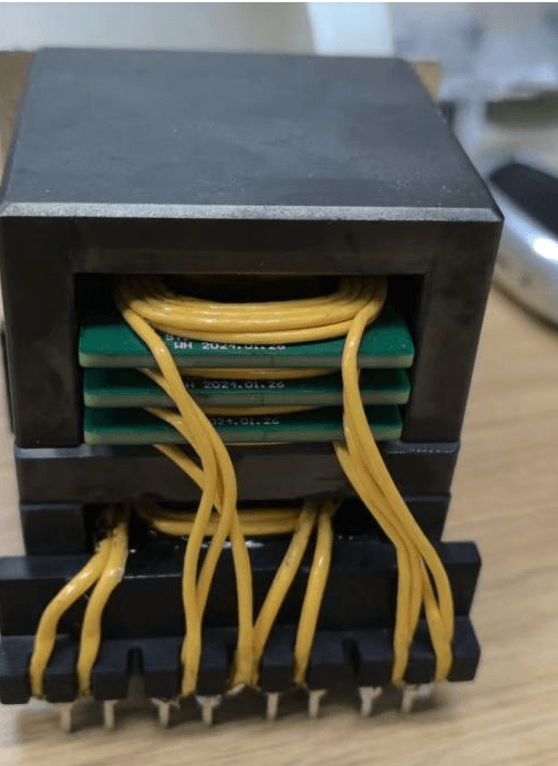
A new type of PCB-wound transformer
According to Mr. Liu, the planar transformer engineer who provided the image, this is a magnetically integrated product that combines a transformer and an inductor.
Many domestic transformer companies are producing similar product structures.
Compared to winding magnetically integrated transformers, this product is smaller in size. Furthermore, the PCB + coil design can, to a certain extent, address the increased difficulty of automated winding for winding magnetically integrated transformers.
According to Wang Yao, the current share of planar transformers in practical applications is estimated to be around 50%, and this share is expected to increase to around 70% in the future.
Future Application Potential of PCB Windings
It is worth noting that PCB-wound transformers offer excellent high-frequency performance, which undoubtedly aligns with the widespread use of third-generation semiconductor devices and can help magnetic components address high-frequency losses at megahertz frequencies.
PCB-wound transformers support switching frequencies of 1-10MHz and achieve efficiencies exceeding 95%. Traditional wire-wound transformers are typically limited to operating frequencies below 100kHz.
For example, Huawei’s 5G base station power supplies and AAU power modules utilize PCB-wound transformers to achieve MHz-level isolation and conversion.
The emergence of new materials in the past two years has further enhanced the high-frequency characteristics of PCB-wound transformers.
For example, hydrocarbon resin/ceramic fillers enable GHz-level RF transformers, while nanocrystalline composite materials can reduce high-frequency losses by 30%. These materials have laid the foundation for the application of PCB-wound transformers in high-frequency scenarios. Further high-frequency, low-loss PCB-wound transformers await further exploration by industry engineers.
Conclusion
Through process innovations and material breakthroughs, PCB-wound transformers are rewriting the design rules of power electronics systems. Despite power and cost constraints, their irreplaceable role in high-frequency and miniaturized applications has been fully demonstrated. With the increasing popularity of wide-bandgap semiconductors (GaN/SiC), PCB-wound technology is expected to become a core pillar of the next generation of efficient energy systems.