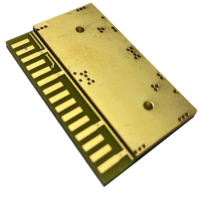
Copper core PCB manufacturing
As electronic devices evolve towards higher power and smaller sizes,Andwin ,with its superior copper core PCB manufacturing technology,has become a key player in solving the heat disspation and performance optimization challenges facing the electronics industry.
In today’s era of rapid development of high-power electronic devices,ensuring stable operation ,efficient heat dissipation,and extend service life has become a common challenge facing the industry,Copper core PCBs,with their superior conductivity ,heat dissipation,and mechanical strength,have become a core solution for power suppliers,new energy,automotive electronics,and other fields.
As a leading manufacturer in this field,Andwin provides high performance copper core PCB products to a wide range of industries through technological innovation and precision craftsmanship.
1 Core Advantages of Copper Core PCBs
Copper core PCBs generally refer to a type of metal core PCB,cosisting of copper foil,an insulating and thermally conductive layer,and a metal base(typically copper).
Compared to traditional FR4 boards,copper substrates offer higher thermal conductivity,typically exceeding 200W/mk,with some products reaching 386386W/(m·K).This significantly improves heat dissipation effeciency compared to standard FR4 boards.This helps quickly dissipate the significant heat generated by the power amplifier chip during operation,preventing overheating and failure.
Copper substrates excel in current carrying capacity,They support ultra-thick copper layers from 2oz to 20 oz,increasing current carrying capacity by over 300%,easily handing high-current scenarios.3oz copper foil (105μm) offters approximately 60% lower trace resistance than 1 oz copper foil,stably carrying continuous current exceeding 30A and even short-term peak currents of 100A.
The copper substrate also offer high rigidity and strength,enhancing the mechanical stability of the circuit board.The bonding strength of the thick copper to the substrate exceeds 1.8N/mm.After 1000 cycles of thermal shock(-40°C to 125°C),the trace breakage rate is less than 0.1% far superior to standard PCBs.
2.Andwin’s Technological Innovation and Manufacturing process
Andwin’s technological innovations in copper core PCB manufacturing are remarkable,The company utilizes”Muti-layer Thick Copper overlay Technology”.which achieves ultra-thick copper layer without delamination through a special lamination process,ensuring high reliability.
This technology addresses the issues of reduced etching accuracy and uncontrolled line width and spacing cause by increased copper thickness in traditional processes.
In terms of”Drilling and copper plating”,Andwin utilizes a deep-hole copper plating process,achieving copper thickness uniformity exceeding 90% within the holes and preventing localized overheating caused by current concentration,For thick metal,the company utilizes high-precision CNC or laser machining to avoid burrs and hole wall damage.
Andwin has also introduced”Non-Destructive copper Treatment”,which coats the copper surface of the substrate with a non-destructive copper film.This film is formed by applying a 5±1.5% concentration of non-destructive copper concentration of non-destructive copper connector solution to the copper surface at a temperature of 25-30°C and allowing it to react for 30-60 seconds.It effectively reduces signal loss on PCBs and improves the copper foil’s peel strength.

3.Application Areas and Success Stories
Copper core PCBs are particularly prominent in the new energy vehicle sector.Core component such as motor controllers and on bo-board chargers(OBCs)rely on their high-current transmission capabilities.
For example,an 800V high-voltage platform OBC uses 6oz thick copper PCBs, enabling power output exceeding 30kw and boosting charging efficiency to over 96%.A Leading new energy vehicle manufactures uses 10oz thick copper PCBs to address temperature rise issues under high currents and ruduce failure rates by 60%.
In the industrial control sector,thick copper PCBs are widely used in high-power inverters and servo drives,resistant to the strong electromagnetic interference and temperature fluctuations of industrial environments.A certain brand’s 15KW inverter,after adopting thick copper PCBs,saw a 40% reduction in failure rates.Customized copper substrates help equipment operate continuously for 100.000 hours without degradation,resulting in a customer repurchase rate exceeding 80%.
The new energy and aerospace sectors have also benefited from copper core PCB technology.In energy equipment,photovoltaic inverters and power storage converters(PCS) utilize thick copper PCBs for efficient power conversion.
The 100kw-class photovoltaic inverter adopts a 4oz thick copper design,reducing power loss by 8% and increasing annual power generation by approximately 2000kWh.The aerospace industry demands extremely high reliability,and thick copper PCBs are used in airborne power supplies and radar systems.They maintain stable operation in extremes.They maintain stable operation in extreme temperatures ranging from-55°C to 125°C,meeting the requirement of the MIL-STD-883 military standard.
4.Quality Assurance and Future Outlook
Andwin has established a comprehensive quality assurance system.The company boasts a CNAS-Certified laboratory and fully automated production capacity exceeding 500.000 square meters.Its clients include Fortune 500 companies such as Huawei ,BYD,and Siemens,and the company is certified by international standards such as ISO9001 and IATF 16949.
The breakdown voltage is ≥3kV, and the insulation layer is filled with high-thermal-conductivity ceramic to ensure safety.The wide operating temperature range of -50°C to 150°C ensures stable operation and adaptability to extreme environments.
As power density requirement increase across application,copper core PCBs are evolving towards thicker thicknesses and finer circuitry.
In area such as high-voltage platforms for new energy vechicles and high-power devices for the industrial internet of Things,the performance advantage of copper core PCB are gradually being transformed into product competiviend,driving related industries towards higher efficiency and miniaturization.The deep integration of performance and application has also made copper core PCBs a key component of high-end electronic devices.
In the future,Andwin will continue to explore hybrid strategies using thick copper and buries copper blocks,and may even transition to metal or ceramic substrates to meet more stringent heat dissipation requirements ,with the rapid development of 5G,the Internet of Things,and artificial intelligence technologies,copper core PCBs will find even greater application in emerging fields such as high-frequency power amplifier circuits.
With the rapid development of 5G,the Internet of Things,and artificial intelligence technologies,Andwin’s copper core PCB solutions will continue to empower a wide range of industries.
The use of copper core PCBs in the OBCs of 800V high voltage platform new energy vehicles can boost charging efficiency to over 96%.A thick copper design for photovoltaic inverters can reduce power losses by 8%,significantly increasing annual power generation.These are all made possible by copper core pcb technology.
In the future,Andwin will continue to explore hybrid strategies using thick copper and buried copper blocks,and even develop metal or ceramic substrates to meet even more stringent heat dissipation requirements.