The invisible city:PCB design:how to Build the Skyscraper of the Electronic World on a single Board
Have you ever wondered what”magic”makes these devices work so precisely when you swipe your phone screen,tap your computer keyboard,or power up your smart home appliances?The answer lies line and myriad of tiny components.It’s printed circuit board(PCB).
But PCBs aren’t born that way.They’re the product of sophisticated and complex design process-:”PCB design”.It’s like planning a fully functional,efficient miniature city on a limited canvans.
Chapter 1:What is a PCB ?Why is it necessary to design one?
Imagine a city without road(wires)connecting all the buildings(electronic components).Without power and information,the city would be a dead city.The PCB is the planning and infrastructure of this “city”.
Original State: A bare insulating board (usually firberglass,or FR4).Design Goal:Plan precise”foundations”(pads)of dozens,hunderds,or even thousands of electronic component(such as resistors,capacitors,and chips)on this circuit board,and connect them safely and efficiently using”copper roads”(conductors)according to circuit logic.Why can’t we just draw randomly?If roads (conductors) arbitraily cross,it will cause”short circuit”(traffic jam);if power lines are too thin,it will cause”power shortages”(traffic jams);if high-speed signal lines take long detours,it will cause signal delays and distortion(information transmission errors).Therefore,PCB design is the prerequisite for ensuring the stable and reliable operation of electronic devices.
Chapter 2:The PCB Designer’s “Blueprint”and”Toolbox”
PCB designers are like the architects and master planners of a city.Their work begins with a “city plan”-the “circuit schematic”.
1.Schematic:This is a logical diagram of the circuit,using symbols to represent each component and lines to show the connections between them.It answers the question,”Who needs to be connected to whom”?
2.PCB Design Software:The designer’s”magic brush”Commonly used software includes Altium Designer,Cadence Allegro,and KiCad(open source and free).These software programs import schematic information and perform layout and routing on a virtual PCB.
Chapter 3:From Zero to One,the Core steps of Building a PCB”City”
Step1:Layout-Giving Components a “Home”
“Core Principles”:Functionally related,high-speed,and heat-generating component should be placed close together,interface components(such as USB ports)should be placed at the edge of the board and heat disspitation and electromagentic compatibility should be considered.
Using city planning:Place the municipal government(main chip),power plant(power module),and data center(memory) in the central area;place the train station(external interfaces)at the city’s edge:and keep industrial areas(heat-generating components) away from residential areas (sensitive signals).
Step 2:Routing-laying the”city road network”
This is the most time-consuming and technically demanding step.Designers use copper traces to connect all pads according to the schematic.
Roads”have different levels:
Power line:Like a city’s main roads,they need to be wider to carry high currents.
Ground line:Like a city’s drainage system,they need to cover a large area to ensure stability and shield against interference.
Signal line:Like ordinary streets,they have high-speed lines(such as USB and HDMI)should be as short and straight as possible,like highways,and avoid sharp turns.
Challenges and Tips:
Avoiding “traffic jams(crosstalk):
Sensitive signal line should be kept separate or isolated with ground traces.
“Solving overpasses”:Single-sided board wiring is like drawing roads on a flat surface;they cannot cross.The solution is to use “vias”-“tunnels”drilled between PCB layers-that allow wires to pass from the top to the bottom of the board,creating overpass-like crossings.Modern,complex PCBs are often multilayer boards,with multiple wiring layers like an”overpass network”.
Step 3:Production Delivery-Transforming the Blueprint into Reality
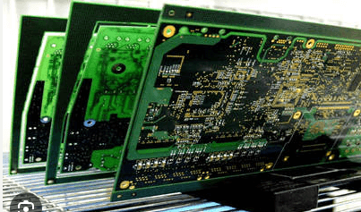
After the design is complete,the designer will output a set of standard”construction documents”(Gerber files)and send them to the PCB fabricator.The fabricator,like developing a photograh,uses processes such as photolithography,etching,drilling,and electroplating to transform the computer design into a physical circuit board.
Chapter 4:Advanced”Urban Planning”-When circuits Become Extremely Complex”
As electronic product become increasingly smaller and more powerful,PCB design faces significant challenges,giving rise to many advanced technologies:
High-density interconnection: Routing hundreds of wires within a space the size of a fingernail requires cutting-edge technologies such as microvias and blind vias.
High-speed digital design: When processing gigahertz-level signals, conductors are no longer simple “wires” but “transmission lines.” Designers must consider impedance matching to prevent signal reflections, much like ensuring uniform pipe thickness to prevent water splashing.
Electromagnetic compatibility design: Ensuring that electromagnetic interference emitted by a device does not affect other devices while also resisting external interference. This is like building a “soundproof wall” for a city.
Power integrity design: Ensures that when a chip demands a huge current instantaneously, the power supply system can respond as quickly as a supercapacitor, preventing voltage drops that could cause system crashes.
Conclusion: Bridging Virtual and Reality
PCB design is an art that blends electronic engineering, physics, and materials science. It’s a bridge between the circuit ideas in an engineer’s mind (the virtual world) and the physical products we touch and use (the physical world).
Every electronic device you use embodies the wisdom and dedication of PCB designers. The next time you tear open an old device and see that delicate green board, take a closer look—the crisscrossing lines aren’t just copper wires, but the traces of
human ingenuity, the invisible, magnificent city that builds our modern digital civilization.