
7 Double-Sided Aluminum MCPCB Design Considerations & Layout Tips
Hardware engineers and PCB layout designers often face sleepless nights over thermal management. You have painstakingly routed a beautiful, high-density power module, but if the heat cannot escape—or worse, if a thermal via accidentally shorts to the metal substrate—your board is dead on arrival.
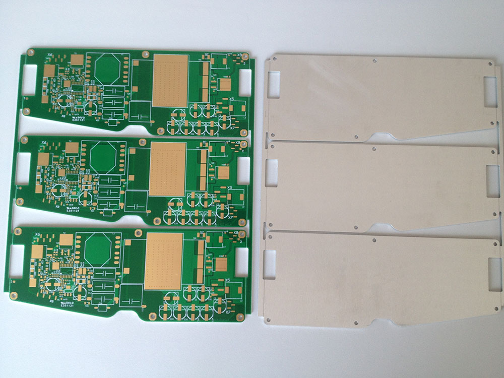
When transitioning from standard FR4 or single-sided boards to double-sided aluminum substrates, the layout rules change drastically. Designing a double-sided metal core board is not just about routing traces on two layers; it is an intricate balancing act between maximizing thermal dissipation, maintaining strict electrical isolation, and navigating complex manufacturing constraints.
In this comprehensive guide, we will break down the critical design considerations for double-sided aluminum boards, translate complex IPC standards into practical layout rules, and provide actionable strategies to ensure your next high-power design is both thermally efficient and highly manufacturable.
Understanding Double-Sided Aluminum MCPCBs: The Basics
In the realm of power electronics, automotive EV controllers, and high-power LED lighting, heat is the ultimate enemy of component longevity. Traditional FR4 boards act as thermal insulators, trapping heat and causing premature component failure. While single-sided metal boards solve basic cooling needs, modern high-density designs require routing on multiple layers.
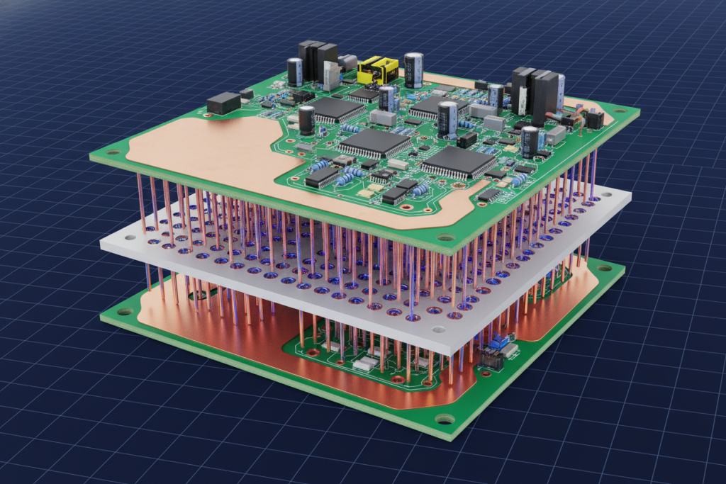
This is where the double-sided Metal Core PCB becomes indispensable. Unlike a standard 2-layer FR4 board, a double-sided aluminum PCB typically features copper trace layers on both the top and bottom, with a solid block of aluminum sandwiched in the middle (or sometimes at the bottom with two copper layers stacked above it).
Why is this topic causing anxiety among layout engineers?
The primary challenge lies in the vias. To connect the top copper layer to the bottom copper layer, you must drill a hole through the aluminum core. If the copper plating inside that via touches the raw aluminum, it creates a catastrophic electrical short. Mastering the isolation techniques, managing the dielectric layer, and adhering to strict clearance rules are what separate a successful production run from a costly batch of scrap.
Core Concepts Simplified
Before diving into the layout software, it is crucial to understand the physical materials and manufacturing processes that dictate your design rules. Let us break down the heavy industry jargon into plain English using practical analogies.
- Dielectric Thermal Conductivity (The Gatekeeper): This is measured in W/m·K (Watts per meter-Kelvin). It represents how fast heat can travel through the insulating layer between your copper traces and the aluminum core. Think of it as a gatekeeper: a higher number means the gate is wider, allowing heat to escape faster. However, highly conductive dielectrics are often stiffer and more expensive.
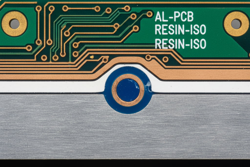
- Resin Plugged Vias / POFV (The Moat): To route a signal through the aluminum core safely, manufacturers use a “drill-fill-drill” process. They drill a large hole, fill it with insulating epoxy resin, and then drill a smaller hole through the center of that cured resin. This creates an insulating “moat” around your conductive via, ensuring the electrical signal never touches the metal core.
- Prepreg (The Glue): This is the fiberglass layer soaked in resin that bonds the copper foil to the aluminum base. It must be thin enough to transfer heat but thick enough to prevent high-voltage electrical arcing.
- Creepage Distance (The Spark Gap): Defined by IPC-2221, this is the shortest path along the surface of the PCB between two conductive parts. Imagine a spark trying to crawl across the surface of the board; you must keep traces far enough apart so the spark cannot make the jump, which is especially risky on metal-backed boards where the substrate itself is conductive.
Concept Comparison: Standard FR4 vs. Double-Sided MCPCB
| Feature | Standard FR4 (2-Layer) | Double-Sided Aluminum MCPCB | Design Impact |
|---|---|---|---|
| Thermal Conductivity | ~0.25 to 0.4 W/m·K | 1.0 to 8.0+ W/m·K | MCPCB handles significantly higher power loads without localized hot spots. |
| Via Architecture | Simple mechanical drill & plate | Complex “Drill-Fill-Drill” isolation | MCPCB vias require much larger annular rings and clearances. |
| Z-Axis Expansion | High (risk of via cracking) | Low (matches metal core better) | Improved reliability in high-temperature cycling environments. |
| Routing Density | Very High | Moderate to Low | You cannot pack vias tightly on an MCPCB due to the resin isolation moat requirement. |
Step-by-Step Guide & Layout Tips
To ensure high manufacturing yields and zero thermal failures, your PCB layout must respect the physical limitations of metal core fabrication. Here are the step-by-step considerations for designing a robust double-sided aluminum board.
Optimizing the Stack-up and Dielectric Selection
The dielectric layer is the most critical material choice in your design. A thinner dielectric layer allows heat to transfer to the aluminum core more rapidly, but it drastically increases the risk of high-voltage breakdown (electrical shorts).
When reviewing the 2-layer aluminum PCB manufacturing process, you will notice that finding the “sweet spot” is essential. For most standard power applications (like LED arrays or moderate motor drives), a dielectric with a thermal conductivity of 1 to 3 W/m·K offers the best balance between cost, thermal performance, and electrical isolation (dielectric strength).
Dielectric Specification Guide for Decision Makers:
| Application Scenario | Recommended W/m·K | Dielectric Thickness | Voltage Breakdown (Typical) | Cost Implication |
|---|---|---|---|---|
| General LED Lighting | 1.0 – 1.5 W/m·K | 75µm – 100µm | ~3000V AC | Low |
| Automotive Power Modules | 2.0 – 3.0 W/m·K | 100µm – 125µm | ~4000V AC | Medium |
| High-Power EV Controllers | 5.0 – 8.0 W/m·K | 125µm – 150µm | >5000V AC | High (Requires specialized ceramic-filled resins) |
Actionable Tip: Always request the material datasheet from your fabricator before routing. Ensure the Dielectric Breakdown Voltage (measured in kV/mm) exceeds your maximum operating voltage by a safety margin of at least 200%.
Thermal Via Placement and Isolation (The “Moat” Technique)
One of the most common reasons double-sided MCPCB designs get rejected during the CAM (Computer-Aided Manufacturing) review is improper via sizing.
Because of the resin isolation process, you cannot use standard FR4 via sizes. If you want a finished via hole of 0.3mm, the manufacturer might need to drill a 0.8mm hole in the aluminum core first to create the resin “moat”.
Standard Routing Rules for MCPCB Vias:
- Minimum Finished Hole Size: Typically 0.3mm to 0.5mm.
- Isolation Clearance: The distance from the edge of the plated via to the raw aluminum core must be at least 0.25mm to 0.3mm.
- Via Spacing: Do not cluster vias tightly. Leave at least 1.0mm pitch between vias to ensure the structural integrity of the aluminum core isn’t compromised by too many large isolation holes.
Smart Component Placement and Copper Pouring
Treat large copper pours on your PCB as “heat sponges”. Copper is an excellent conductor of heat. Before the heat even attempts to cross the dielectric layer into the aluminum core, a large copper pour can soak up the localized heat from a hot component (like a MOSFET or high-power LED) and spread it laterally across the surface of the board.
- Avoid Hotspot Clustering: Never place your hottest components right next to each other. Spread them evenly across the board to utilize the entire surface area of the aluminum core.
- Maximize Copper Pours: Use polygon pours on all unused routing areas on both the top and bottom layers. Connect these pours to your ground net to act as lateral heat spreaders.
- Solder Mask Openings: For extreme heat-generating components, consider leaving the solder mask off the thermal pad area to allow direct heat transfer to a heat sink, though this requires careful handling to avoid oxidation.
High-Voltage Routing: Strict Creepage and Clearance Rules
When dealing with metal core boards, the risk of high-voltage arcing is magnified because the substrate itself is a massive conductive plane. You must strictly adhere to IPC-2221 standards.
- Clearance (Line-of-Sight): The distance through the air between two conductors.
- Creepage (Surface Distance): The distance along the surface of the dielectric.
Because the aluminum core is often grounded, you must calculate the creepage not just between two copper traces, but between the copper trace and the exposed aluminum edge of the board.
Actionable Tip: Keep all copper traces, pads, and pours at least 2.0mm to 3.0mm away from the board edge (the routing outline). When the board is v-scored or routed out of the panel, the cutting tool exposes the raw aluminum. If a trace is too close to the edge, high voltage can arc directly from the trace to the exposed core.
Knowing When to Switch: Alternative Substrate Decisions
Double-sided aluminum is fantastic, but it is not a silver bullet. As a decision-maker, you must know when to pivot to other technologies based on your thermal and electrical data.
- High Current vs. High Heat: If your primary issue is carrying massive amounts of current (e.g., 100 Amps) rather than just dissipating heat from a small footprint, you need thicker copper. Compare your options by reading about Heavy Copper PCB vs Metal Core PCB to see which architecture handles I²R losses better.
- Extreme Temperatures: Aluminum begins to warp and lose its mechanical properties at extremely high temperatures. If your operating environment exceeds 150°C consistently, you should evaluate Ceramic PCB vs Metal Core PCB. Alumina or Aluminum Nitride ceramics offer zero warpage and incredible dielectric strength.
- High-Frequency / RF Applications: Aluminum boards typically use dielectrics with high Dk/Df values, which ruin high-speed signal integrity. If you are designing a high-power RF amplifier that needs both cooling and signal integrity, look into a Rogers 4350B Copper Core PCB which pairs a high-frequency laminate with a solid metal backing.
Expert Tips & Common Pitfalls to Avoid
If you browse engineering communities like r/PrintedCircuitBoard on Reddit, you will quickly notice recurring themes of anxiety and failure regarding metal core layouts. Here are the most common pitfalls based on real-world manufacturing experience, and how to avoid them.
Pitfall 1: Ignoring the “First Drill” Size Constraints
Many designers treat MCPCB vias like FR4 vias, placing them tightly together under a BGA or power pad. They forget that the manufacturer must drill a massive isolation hole first. If vias are placed too close, the isolation holes overlap, completely destroying the aluminum core in that area and causing the board to physically snap or warp during fabrication.
The Fix: Always use a minimum via pitch of 1.0mm to 1.5mm on double-sided MCPCBs.
Pitfall 2: Unbalanced Copper Causing the “Potato Chip” Effect
Metal core boards are susceptible to warpage during the high-heat lamination process. If you have a massive solid copper pour on the top layer, but only a few thin traces on the bottom layer, the differing rates of thermal expansion will cause the board to bow like a potato chip.
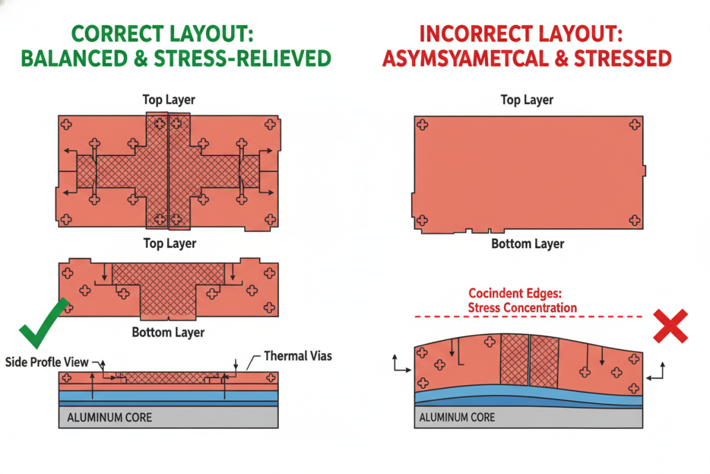
The Fix: Always balance your copper. If you have a 90% copper fill on the top layer, use a cross-hatched copper pour on the bottom layer to achieve a similar copper density, even if it is just a dummy ground plane.
Pitfall 3: Inadequate Edge Clearance
As mentioned earlier, routing traces right up to the board edge is a guaranteed way to cause a short circuit. When the V-cut blade scores the board, it displaces the metal. If the clearance is too small, the displaced aluminum burr will touch the copper trace.
The Fix: Implement a strict keep-out zone of at least 2.5mm from all board edges and non-plated mechanical holes.
Conclusion & Final Thoughts
Designing a double-sided aluminum MCPCB requires a fundamental shift in how you approach PCB layout. By understanding the mechanical reality of the dielectric “gatekeeper” and the via isolation “moat,” you can design boards that not only survive massive thermal loads but also sail smoothly through the manufacturer’s DFM (Design for Manufacturing) checks.
Remember to leverage large copper pours as lateral heat sponges, strictly enforce your IPC-2221 creepage distances, and always balance your copper to prevent warpage.
Quick Summary Guide for Layout Engineers
| Design Parameter | Standard FR4 Rule | Double-Sided MCPCB Rule | Why It Matters |
|---|---|---|---|
| Via Pitch (Spacing) | 0.5mm+ | 1.0mm – 1.5mm+ | Prevents overlapping of the large resin isolation holes. |
| Edge Clearance | 0.2mm – 0.5mm | 2.5mm – 3.0mm | Prevents high-voltage arcing to the exposed raw aluminum edge. |
| Copper Balance | Recommended | Strictly Mandatory | Prevents board warpage (bow and twist) during lamination. |
| Thermal Reliefs | Use on all ground pins | Avoid on high-power pins | Solid connections to copper pours maximize lateral heat spreading. |
If you are ready to move your high-power design into production, or if you are still debating which substrate technology fits your thermal budget, consult with your fabrication partner early in the design phase. Getting the stack-up right on day one will save you weeks of redesign headaches later.
Frequently Asked Questions
Q1: What is a double-sided aluminum MCPCB?
A: It features copper trace layers on both top and bottom with an aluminum core sandwiched in between, offering superior thermal conductivity compared to standard FR4.
Q2: How do vias avoid shorting to the aluminum core?
A: Manufacturers use a drill-fill-drill process with epoxy resin to create an insulating “moat” around plated through-holes, ensuring electrical isolation from the conductive metal core.
Q3: What is the minimum via spacing on double-sided aluminum boards?
A: Use a minimum via pitch of 1.0mm to 1.5mm to prevent overlapping isolation holes that could compromise the aluminum core structure.
Q4: Why is edge clearance critical on metal core PCBs?
A: Traces must stay 2.5mm to 3.0mm from board edges to prevent high-voltage arcing to exposed aluminum during V-scoring or routing.
Q5: How do I prevent board warpage?
A: Balance copper density between top and bottom layers. If one side has heavy copper pours, match it with similar copper coverage on the opposite side.
Q6: When should I choose ceramic or heavy copper instead of aluminum?
A: Choose ceramic for temperatures exceeding 150°C, heavy copper for extremely high current carrying, and Rogers laminates for high-frequency RF applications.