
PCB Thermal Management: Techniques Beyond Metal Core PCB
When a 15W power module failed thermal testing at 85°C, the engineering team discovered their metal core PCB couldn’t handle heat from densely packed components. The solution wasn’t switching to ceramic substrates—it was implementing thermal vias, copper pours, and optimized component placement on standard FR4.
Metal core PCBs excel in LED and power applications, but modern high-density designs demand comprehensive thermal strategies. This guide covers proven techniques that work across FR4, multilayer boards, and specialized substrates, helping you prevent thermal failures before production.
Heat Transfer Fundamentals in PCB Design
PCB thermal management relies on conduction, convection, and radiation working together. Conduction moves heat through copper traces and planes. Convection transfers heat to air or coolant. Radiation contributes minimally in most electronics.
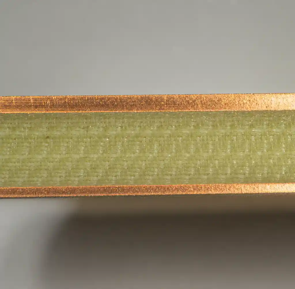
Standard FR4 has thermal conductivity of 0.3-0.4 W/mK, while copper conducts at 385 W/mK—nearly 1000× better. This explains why copper geometry dominates thermal performance. Designers must create intentional heat paths using copper features rather than relying on substrate properties.
Thermal resistance (θ) quantifies heat transfer from junction to ambient. A typical power IC on FR4 without thermal management shows 40-60°C/W resistance. Adding thermal vias and copper pours reduces this to 15-25°C/W, often eliminating metal core requirements.
| Thermal Method | θJA Reduction | Cost Impact | Applications |
|---|---|---|---|
| Thermal vias (0.3mm) | 40-50% | Low | All PCB types |
| Heavy copper (2oz) | 25-35% | Medium | FR4 boards |
| Metal core substrate | 60-70% | High | LED, power |
| Ceramic substrate | 70-80% | Very high | RF, automotive |
Thermal Via Implementation Strategy
Thermal vias create vertical heat pipes through PCB layers, connecting components to internal planes and bottom-side cooling. A 0.3mm via with 1oz plating offers 0.35°C/W thermal resistance. Designers need 10-20 vias under power components for meaningful temperature reduction.
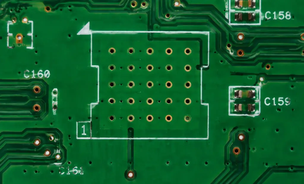
Position vias directly under QFN and DFN thermal pads. For BGAs, place vias between solder balls. Avoid vias under small pads where solder wicking causes unreliable joints. Use 0.5-0.7mm via spacing for optimal density without manufacturing complications.
Filled vias improve performance by 15-20% versus unfilled, though cost increases. Specify via filling for components dissipating over 5W. Connect via arrays to ground or power planes with maximum copper area—a via dumping heat into narrow traces wastes thermal potential.
Copper Pour Design for Heat Spreading
Copper pours transform unused board area into thermal infrastructure. These large regions spread heat laterally, reducing hot spots. Specify 2oz copper for thermal-critical designs—it conducts twice the heat of standard 1oz copper for only 20-30% cost increase.
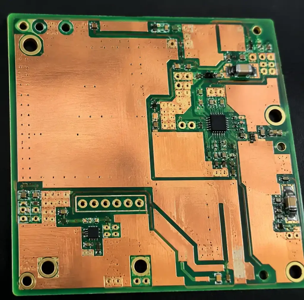
Position pours around heat-generating components, extending 10mm beyond component outlines. Connect to thermal vias penetrating internal planes. In multilayer boards, preserve plane integrity by routing signals on dedicated layers rather than interrupting thermal planes.
Internal planes should maintain continuous copper. Every routing cutout creates thermal resistance. Some designs dedicate complete layers as uninterrupted thermal planes, especially in 6-layer constructions where layer count enables separation of thermal and signal functions.
Thermal Relief Considerations
Thermal reliefs ease hand-soldering by limiting heat flow into copper planes. For power components, these spoke patterns sabotage thermal performance. Override thermal relief settings on power IC pads, using solid copper connections instead.
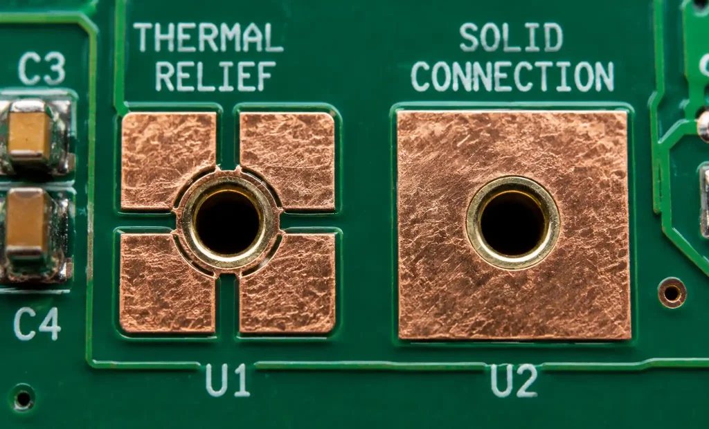
Apply thermal reliefs selectively. Low-power logic benefits from thermal reliefs. Power regulators and MOSFETs need solid connections. Reflow soldering handles solid connections well. Hand-soldering requires high-wattage irons (60-80W) and longer dwell time.
Component Placement for Thermal Optimization
Component placement establishes thermal management foundation. Poor placement creates unsolvable problems regardless of substrate choice. Separate high-power components by 10-15mm minimum—clustering creates thermal interaction where each device elevates ambient temperature for neighbors.
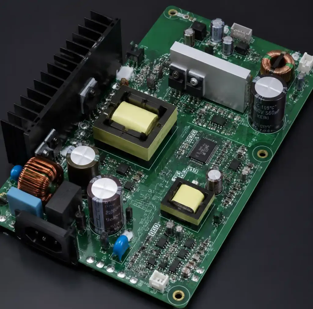
Position power components near board edges for heat transfer to enclosures or chassis. Center-board placement traps heat in FR4 with limited escape paths. Reserve 20-25mm radius around heat-sinked components for mounting hardware clearance.
In vertical orientations, arrange components for natural convection—hot air rises. Avoid positioning components directly above heat sources where exhaust air preheats incoming devices.
| Power Level | Spacing | Position | Heat Sink |
|---|---|---|---|
| < 1W | 5mm | Any | Not needed |
| 1-3W | 10mm | Prefer edges | Optional |
| 3-10W | 15mm | Edge mount | Recommended |
| > 10W | 20mm+ | Edge + vias | Required |
Active Cooling Integration
Forced airflow reduces component temperatures by 15-25°C. A 40mm fan moving 5 CFM costs $2-5 but extends thermal capacity significantly. Design clear airflow paths with intake and exhaust openings. Position heat-generating components in primary airflow.
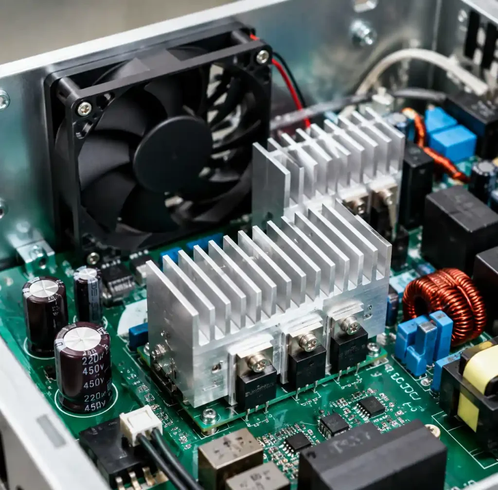
Heat sinks increase surface area by 10-20× compared to package surfaces. Aluminum extrusions attach via clips or thermal adhesive. Use thermal interface materials (TIM) to minimize contact resistance—phase change materials, thermal pads, or paste each suit different applications.
Liquid cooling handles extreme power densities above 100W per board. Cold plates extract heat through circulation. Implementation cost restricts this to specialized high-power applications like AI accelerators and RF power amplifiers.
Thermal Simulation Workflow
Thermal simulation predicts temperature distribution before prototyping. Modern PCB design tools integrate solvers analyzing conduction, convection, and radiation based on board geometry and component power.
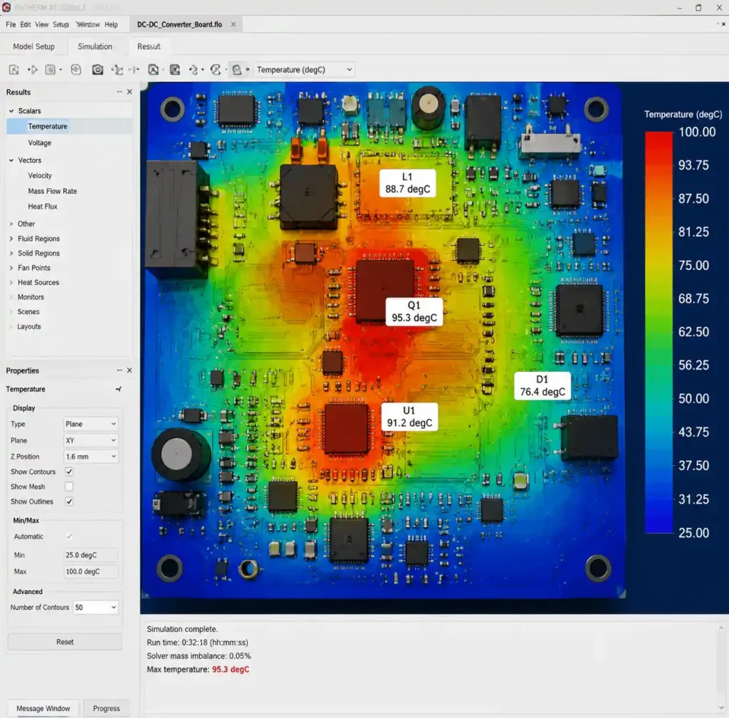
Input accurate power dissipation from datasheets—typical and maximum under expected conditions. Model boundary conditions: ambient temperature, airflow velocity, enclosure materials. Set conditions matching deployment environments, not idealized free air at 25°C.
Validate simulations with prototype measurements using thermocouples or thermal cameras. Expect 10-15% deviation between prediction and reality. Common pitfalls include ignoring thermal vias, oversimplifying copper geometry, and using default material properties.
Advanced Materials for FR4 Construction
Thermally enhanced FR4 achieves 0.6-1.0 W/mK using ceramic fillers—double standard FR4 performance while maintaining processing compatibility. Consider for multilayer boards where internal planes need better thermal coupling between layers.
Copper coin technology embeds thick copper slugs in routed cavities beneath power components. These create localized thermal mass superior to standard foil, costing less than metal core substrates while providing comparable performance in concentrated areas.
Thermal interface materials between PCB and enclosure complete heat paths. Gap pads, phase change materials, and graphite sheets fill air gaps with 3-8 W/mK conductivity. Select TIM matching application temperature range and compression requirements.
| Enhancement | Thermal Gain | Cost | Complexity |
|---|---|---|---|
| Enhanced FR4 | 2× standard | +10-15% | Standard process |
| 2oz copper | 2× vs 1oz | +20-30% | Standard fab |
| 3oz copper | 3× vs 1oz | +40-60% | Capable fab needed |
| Copper coin | 5-8× local | +30-50% | Specialized process |
Multilayer Thermal Management
Four-layer stackups (Signal-Ground-Power-Signal) dedicate two internal planes for ground and power. These uninterrupted layers create low-resistance thermal paths between surfaces. Thermal vias from components through planes to bottom copper enable heat extraction without routing constraints.
Six-layer boards add signal layers while maintaining plane integrity. Signal routing occurs on dedicated layers, leaving thermal planes uncompromised. Via transitions introduce 0.1-0.3°C/W resistance—minimize transitions in thermal paths.
HDI construction with blind and buried vias preserves surface area while creating internal thermal connections. A blind via from top to internal plane extracts heat without consuming bottom area. HDI costs exceed standard vias but provides density advantages in space-constrained designs.
FAQ
What provides the best thermal improvement per dollar?
Thermal via arrays offer maximum cost-effectiveness. Adding 15-20 vias (0.3mm) costs $0.05-0.10 per board but reduces thermal resistance by 40-50%. This often eliminates metal core substrate requirements.
How many thermal vias do I need?
Calculate based on component power and temperature rise. Each 0.3mm via contributes 0.35°C/W resistance. For 5W with 30°C rise allowance, target 6°C/W total resistance, requiring 18-20 parallel vias accounting for via-to-plane connections.
When does metal core justify its cost premium?
When power density exceeds 5W per square inch, substrate thermal conductivity requirements exceed 2 W/mK, or junction temperatures demand maximum performance. LED arrays, power modules, and automotive electronics commonly require metal core where FR4 cannot meet specifications.
Should I remove thermal reliefs from power pads?
Yes, for maximum heat extraction. Thermal reliefs reduce copper connection by 60-80%, creating thermal bottlenecks. Power components need solid connections to vias and pours. Accept more difficult hand-soldering for significantly better thermal performance.
What copper weight for high-power boards?
Specify 2oz copper for components above 3W individually or boards exceeding 15W total. The 30% cost increase delivers 100% conductivity improvement versus 1oz. Reserve 3oz+ for extreme applications over 10W per component or 50W board level.
How do I validate thermal design before prototypes?
Run thermal simulation with accurate component power from datasheets. Model actual enclosure conditions including ambient temperature and airflow. Explicitly model thermal vias and copper geometry. Simulation accuracy typically falls within 10-15% of measurements.
Conclusion
Effective PCB thermal management extends beyond substrate selection. Thermal vias, copper pours, and optimized placement deliver dramatic temperature reductions on standard FR4. These techniques cost-effectively address challenges many assume require metal core or ceramic substrates.
Start with board-level heat paths—via arrays extracting heat from components, copper pours spreading heat laterally, and multilayer construction creating three-dimensional thermal networks. Material enhancements like heavy copper amplify geometric techniques. Active cooling addresses remaining requirements where passive methods reach limits.
Integrate thermal considerations throughout design rather than treating as post-layout problems. Early component placement decisions, copper distribution during routing, and validated simulation prevent costly redesigns. Systematic thermal management reduces junction temperatures by 30-50°C compared to default practices, improving reliability across operating ranges while avoiding expensive specialized substrates.