
Back Drilling PCB Vias: Stub Removal for Signal Integrity
In high-speed PCB design, via stubs are overlooked signal integrity killers. When your SerDes link fails eye diagram compliance at 10 Gbps or DDR4 interface shows unexplained bit errors, the culprit is often a 50-mil via stub resonating at the wrong frequency. Back drilling eliminates these stubs by physically removing unused copper barrel after plating—pushing resonant frequencies beyond your signal bandwidth and recovering insertion loss margins.
What Via Stubs Do to Your Signal
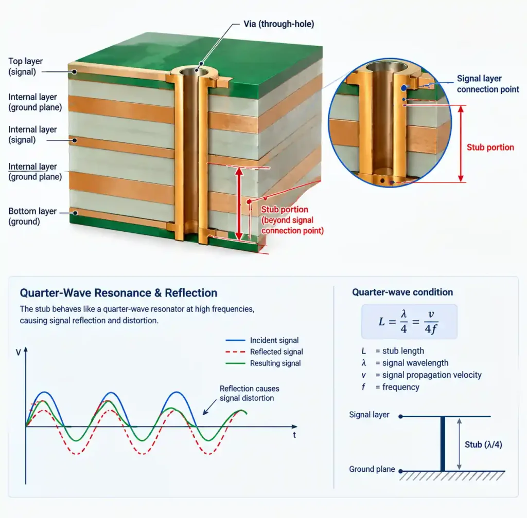
A via stub is the unused portion of a plated through-hole extending past the last connected layer. In a 10-layer board where signal transitions from Layer 1 to Layer 4, the copper barrel from Layer 5 to Layer 10 serves no electrical function—but behaves as an unterminated transmission line stub reflecting signals back into your trace.
The stub’s quarter-wave resonant frequency occurs where electrical length equals λ/4. For a 40-mil stub in FR4 (propagation velocity ≈6 inches/ns), first resonance appears near 9.4 GHz. At this frequency, reflected signal returns 180° out of phase, creating a deep null in insertion loss and degrading eye opening. Additional nulls appear at every odd harmonic.
Signal integrity measurements on DDR4 channels show via stubs cause insertion loss increase of 1-3 dB at frequencies above 5 GHz, with exact degradation depending on stub length and impedance mismatch. When your operating frequency or its significant harmonics land near stub resonance, you see eye closure, jitter amplification, and elevated bit error rates that equalization cannot fully recover.
Back Drilling Process and Depth Control
Back drilling—also called controlled depth drilling—uses a slightly larger drill bit (typically 8-12 mils larger than original via) entering from the board’s opposite side. The drill removes plated copper barrel, stopping within controlled distance of the target layer to leave only functional portion intact.
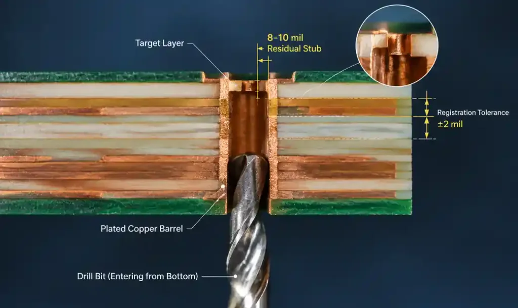
The critical challenge is depth control. The drill must stop 5-15 mils (typically 8-10 mils) before reaching target pad to avoid damaging signal connection. This “back drill residual stub” represents the practical limit—you cannot eliminate stub entirely, but you can reduce it from 50+ mils to under 10 mils, pushing first resonance from 9 GHz to beyond 30 GHz.
Manufacturers use CNC machines with precision depth control and real-time feedback systems following IPC-6012 qualification standards. Process sequence follows plating completion: drill through-hole, plate barrel, verify registration, then back drill from opposite side. Registration accuracy between original drill and back drill operation must stay within ±3 mils to avoid exposing via barrel or leaving excessive stub length.
Typical depth control tolerance is ±5 mils. For target residual stub of 8 mils, actual results range 3-13 mils across the panel. This variability comes from stack-up thickness tolerance, drill bit wear, and material hardness variations.
When Back Drilling Becomes Mandatory
The decision to back drill depends on your signal’s frequency content and insertion loss budget:
| Data Rate | Nyquist Frequency | Via Stub Impact | Back Drilling Required |
|---|---|---|---|
| ≤2.5 Gbps | ≤1.25 GHz | Minimal | No |
| 5 Gbps | 2.5 GHz | Moderate, 0.5-1 dB loss | Consider for ≥10 layers |
| 10 Gbps | 5 GHz | Significant, 1-2 dB loss | Yes for stubs >30 mils |
| 25 Gbps | 12.5 GHz | Severe, 2-4 dB loss | Yes for stubs >15 mils |
| 56 Gbps (PAM4) | 28 GHz | Critical, design-limiting | Yes for all transition vias |
PCIe Gen3 (8 GT/s) can sometimes avoid back drilling with careful via placement and short stubs. PCIe Gen4 (16 GT/s) demands back drilling for layer transitions in boards exceeding 8 layers. PCIe Gen5 (32 GT/s) requires back drilling on virtually all signal vias plus tight residual stub control under 6 mils.
Cost Analysis and Design Trade-offs
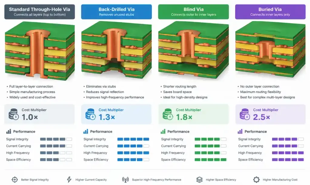
Back drilling adds 15-30% to PCB fabrication cost, depending on board complexity, panel utilization, and via count. For a prototype 12-layer board with 200 signal vias requiring back drilling, expect $400-800 additional cost compared to standard through-holes. Production volumes above 100 panels see this premium drop to 10-20% as setup costs amortize.
| Via Strategy | Fab Cost Multiplier | Routing Density | Signal Performance | Best Application |
|---|---|---|---|---|
| Standard through-hole | 1.0× (baseline) | Low | Adequate <5 Gbps | Cost-sensitive, low-speed |
| Back-drilled PTH | 1.15-1.30× | Medium | Good to 25+ Gbps | High-speed with cost control |
| Blind via (HDI) | 1.8-2.5× | High | Excellent | Dense BGA fanout, mobile |
| Buried via (HDI) | 2.0-3.0× | Very high | Excellent | Extreme density, no via stubs |
Back drilling offers the best cost-performance ratio for signal integrity improvement when you need through-hole reliability but must eliminate stub effects. It avoids sequential lamination cycles required for blind and buried vias while delivering comparable electrical performance for high-speed serial links.
Design Rules for Back-Drilled Vias
Successful back drilling requires design rules accounting for manufacturing tolerances:
Minimum stub length before back drilling: 25 mils. Shorter stubs cannot be reliably back drilled due to registration tolerance and mechanical clearance needs.
Target residual stub: 8-10 mils from back drill to target pad, balancing manufacturing yield against electrical performance.
Via pad size adjustment: Add 8-10 mils to standard pad diameter on the layer where back drilling terminates, providing margin for registration error.
Layer-to-layer transitions: Design signal transitions to land on layers where resulting stub length after back drilling stays under 10 mils.
Aspect ratio limits: Back drilling depth cannot exceed 10:1 aspect ratio (depth:drill diameter). For a 28-mil back drill bit, maximum achievable depth is 280 mils.
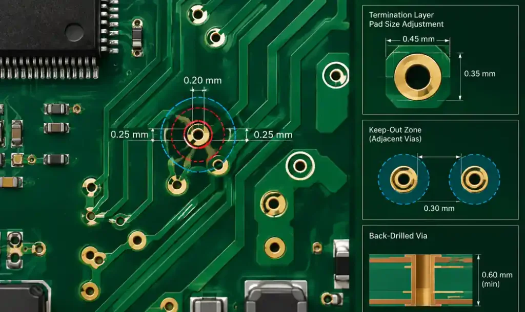
Keep-out zones: Maintain 20-mil clearance between back-drilled vias and adjacent through-holes or blind vias to avoid damaging neighboring structures.
Alternative Solutions and Comparisons
When back drilling isn’t feasible or cost-effective, consider these alternatives:
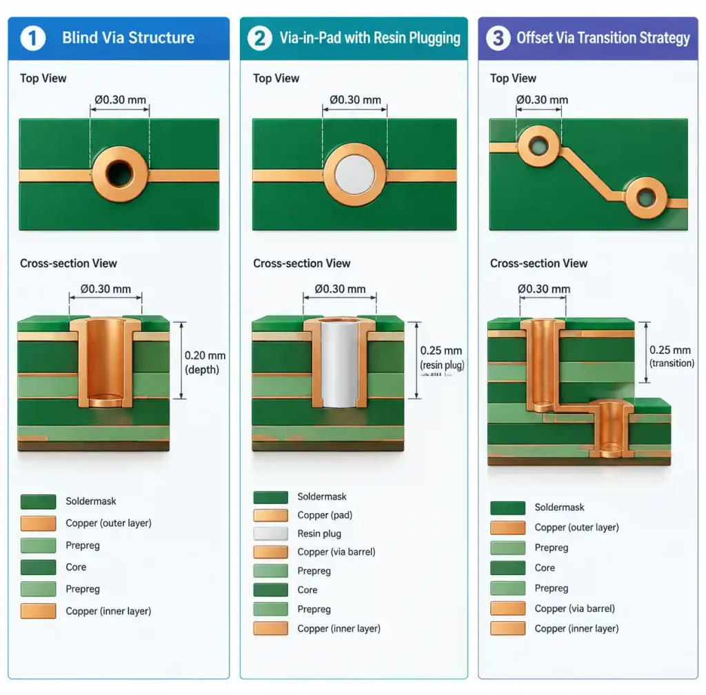
Blind vias: Stop on internal layers without penetrating entire board. A blind via from Layer 1 to Layer 4 has zero stub beyond Layer 4. Cost is 1.8-2.5× standard drilling, requires sequential lamination, and limits you to 1-2 drill-and-plate cycles.
Via-in-pad: Places via directly under BGA pad, then fills with epoxy and caps with copper. This eliminates stub effects by terminating via at pad layer. However, via-in-pad requires resin plugging ($150-300 added cost per panel) and careful planarization to prevent solder joint defects.
Offset via transitions: Route signal to via positioned so stub length naturally stays short. This costs nothing but limits routing flexibility and may force longer trace lengths.
Manufacturing Verification
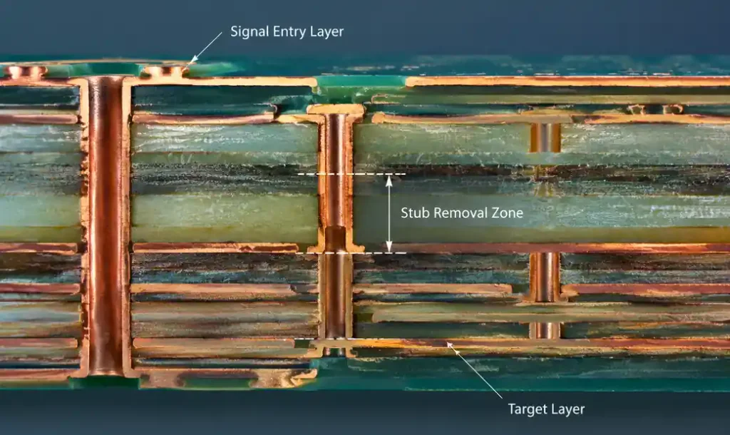
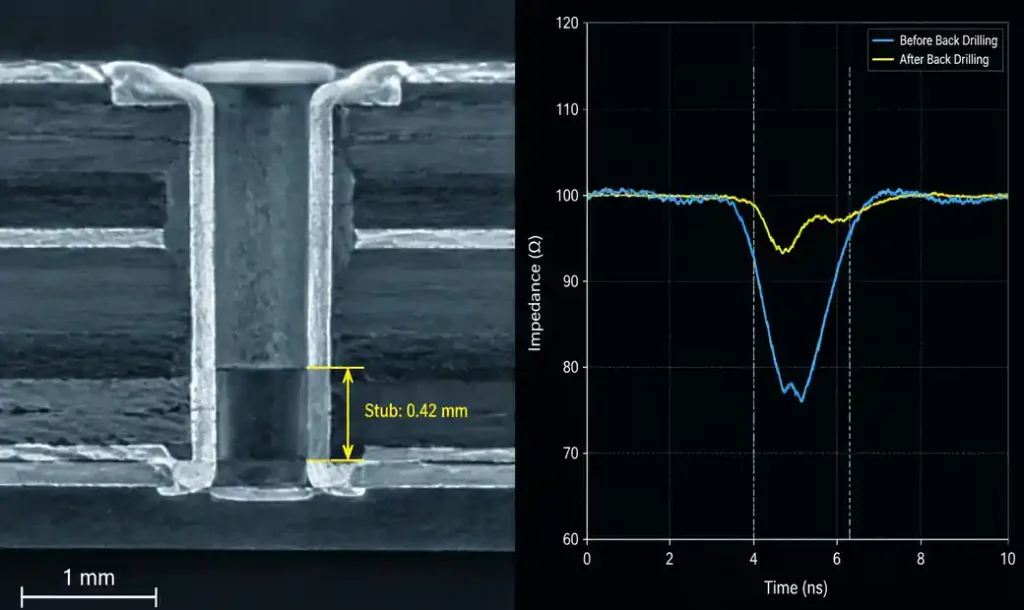
After back drilling, manufacturers verify depth using X-ray cross-section or microsectioning samples from each panel, confirming residual stub length and checking for drill breakthrough.
Time-domain reflectometry (TDR) provides electrical verification of stub removal. A TDR trace shows via as impedance discontinuity; stub appears as smaller reflection following main via discontinuity. Successful back drilling removes this secondary reflection, leaving only via barrel impedance step visible.
For production qualification, request C-SAM (acoustic microscopy) inspection to detect delamination around back-drilled vias, as secondary drilling introduces mechanical stress.
Integration with High-Speed Design
Back drilling integrates with other signal integrity techniques to meet link budgets:
Combine back drilling with controlled impedance design to maintain 50Ω or 100Ω differential impedance through via transition. Via barrel impedance typically drops to 30-40Ω; use anti-pad diameter adjustments to compensate and minimize reflection coefficient.
Use back drilling on signal vias while implementing ground stitching vias (non-back-drilled) to maintain return path continuity. Ground vias don’t carry high-speed signals, so their stubs don’t affect signal integrity, but they must be frequent enough (every 100-150 mils along high-speed traces) to provide low-inductance return paths.
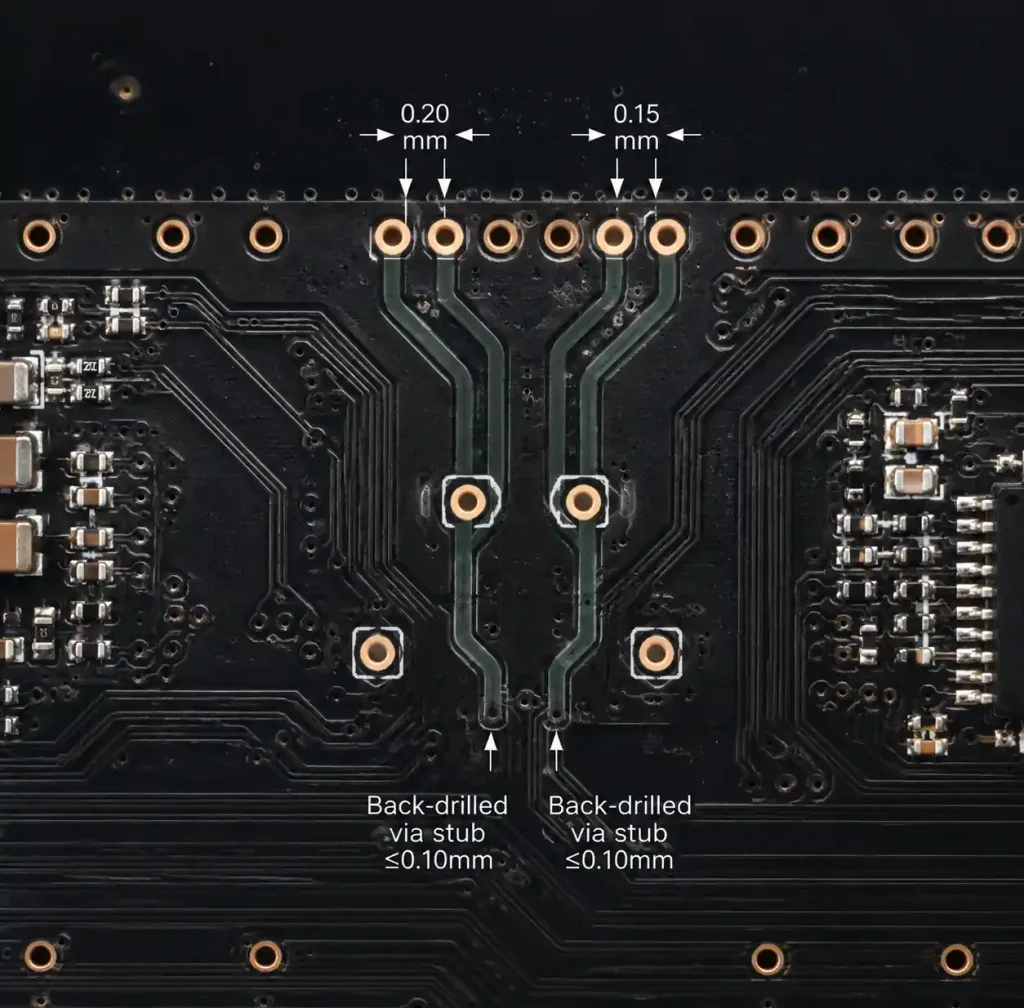
For differential pairs, back drill both vias to identical residual stub lengths. Stub length mismatch between P and N signals converts common mode to differential mode, degrading mode conversion parameters (Scd21).
Common Design Mistakes
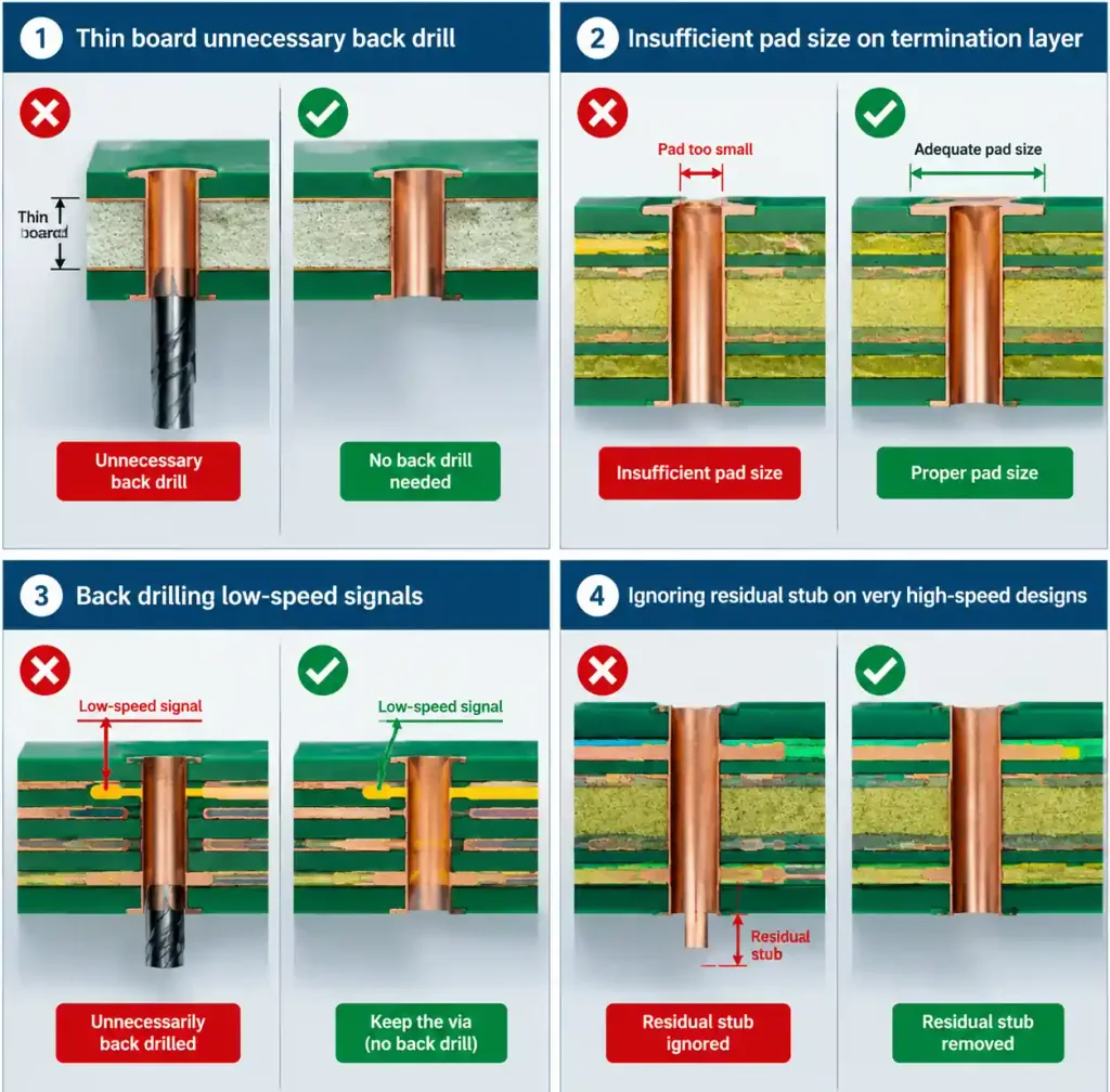
Mistake 1: Specifying back drilling on thin boards (<62 mils). Short total stub length often doesn’t justify cost and manufacturing complexity. Verify via stubs actually resonate within your signal bandwidth before adding back drilling.
Mistake 2: Ignoring residual stub impact. An 8-10 mil residual stub still affects 28+ GHz signals. For 56 Gbps PAM4 designs, even back-drilled vias may require additional optimization.
Mistake 3: Back drilling vias that don’t need it. Only high-speed signal vias require back drilling. Power, ground, and low-speed I/O vias (SPI, I2C, UART) function perfectly with full-length stubs.
Mistake 4: Insufficient pad size on back drill termination layer. Using standard via pad dimensions leads to yield loss when back drill registration varies.
FAQ
Q: Can I back drill from both sides of the board?
A: Yes, dual-sided back drilling removes stubs from both ends of a via when signal path uses only middle layers. This is common in high-layer-count designs (20+ layers) where signals route on internal layer pairs. Cost increases proportionally as you’re running two back drill operations per via.
Q: What happens if the back drill breaks through to the signal layer?
A: Via failure—signal connection is destroyed. This is why manufacturers maintain an 8-10 mil safety margin (residual stub) and why tighter depth control specifications increase cost.
Q: Does back drilling affect via reliability in thermal cycling?
A: No measurable impact. Via barrel plating remains intact and continuous on functional portion. IPC-6012 Class 3 boards with back drilling pass 500+ thermal cycle testing without via failures attributable to back drilling.
Q: Can you back drill microvias or blind vias?
A: No. Microvias (laser-drilled, ≤6 mil diameter) and blind vias are too small and shallow for mechanical back drilling. These via types inherently have minimal or zero stub length by design.
Q: How do I specify back drilling on my fabrication drawing?
A: Add a note: “Back drill [via list or net class] from [top/bottom] to [target layer], target residual stub 8-10 mils.” Include back drill diameter (typically +10 mils over finished hole size) and reference IPC-6012 for workmanship standards.
Q: Does back drilling work with filled vias?
A: Yes, but via fill must use material compatible with secondary drilling. Conductive epoxy fill can be back drilled; solder-filled vias generally cannot due to drill bit loading and thermal stress.
Conclusion
Back drilling transforms standard through-hole vias into signal integrity-compatible structures for multi-gigabit designs without full HDI fabrication cost. By removing unused copper stubs, you push via resonances beyond 25-30 GHz and recover 1-3 dB insertion loss that would otherwise close eye diagrams. The process requires precise depth control, adds 15-30% to fabrication cost, and demands design rules accounting for residual stub length and manufacturing tolerances. For designs above 10 Gbps in boards exceeding 8 layers, back drilling delivers measurable signal integrity improvement at a fraction of blind via costs, making it standard for PCIe Gen4/Gen5, 25G Ethernet, and high-speed SerDes applications.
At Andwin Circuits, we offer back drilling capabilities with residual stub control to 8 mils and registration accuracy within ±3 mils for high-speed PCB manufacturing. Our controlled depth drilling process supports boards from 8 to 40+ layers with verification through X-ray cross-section and TDR testing.