
PCB Routing Complexity: Layer Count Optimization Strategies
Layer count decisions impact 60% of PCB manufacturing costs and directly determine routing success for high-density designs. Engineers face a persistent challenge: adding layers solves routing congestion but increases fabrication costs by 60-80% per additional layer pair, while insufficient layers create unroutable designs that delay product launches by months.
If you want to optimize PCB layer count for your complex routing requirements, you need to understand routing density calculation, component placement strategies, via optimization techniques, and cost-performance trade-offs. This guide provides actionable layer count optimization strategies based on IPC-2221 design standards and real-world manufacturing constraints.
What Drives PCB Layer Count Requirements?
PCB layer count stems from three primary factors: routing density, power distribution requirements, and signal integrity constraints. Routing density measures total net length divided by available routing area per layer, determining whether a given layer count can accommodate all connections at required trace widths and spacing.
High pin-count BGAs are the most common driver forcing high layer counts. Large BGA packages with 500-1500 pins at 0.5-0.8mm pitch require multiple layers just for escape routing—fanning signals from inner pin rows to the package perimeter before general PCB routing begins. A dense BGA with 10 signal rows across the footprint typically requires 5 signal layers minimum for breakout routing alone.

Power distribution networks add complexity beyond signal routing. Modern processors and FPGAs draw 50-200A at sub-1V rails, requiring multiple dedicated power planes with controlled impedance from DC through 500 MHz. High-performance designs routinely dedicate four or more layers exclusively to power distribution, separate from signal routing requirements.
Routing Density Calculation Method
Calculate routing density to determine minimum layer count before layout begins. Count all point-to-point connections and estimate average net length based on component placement. A design with 800 nets averaging 50mm length yields 40,000mm total routing demand.

Calculate available routing area per signal layer. For a 100mm × 100mm board with 30% area consumed by components and vias, each layer provides approximately 7,000mm² usable routing area. With 5mil trace width and 5mil spacing (10mil pitch), each layer accommodates roughly 700,000mm routing capacity.
Divide total routing demand by per-layer capacity: 40,000mm ÷ 700,000mm = 0.057 layers. Apply 50% efficiency factor for routing congestion: 0.057 ÷ 0.5 = 0.11 layers, suggesting 4-6 signal layers minimum. Add 2-4 dedicated power planes for complete layer count estimation.
| Design Complexity | Net Count | BGA Pin Count | Typical Signal Layers | Typical Total Layers |
|---|---|---|---|---|
| Simple (IoT, sensors) | <500 | <256 | 2 | 4 |
| Moderate (Industrial control) | 500-1500 | 256-676 | 4-6 | 6-8 |
| Complex (Automotive ADAS) | 1500-3000 | 676-1156 | 6-10 | 10-14 |
| High-density (AI servers) | >3000 | >1156 | 10-20 | 16-28 |
Component Placement for Routing Efficiency
Strategic component placement reduces required layer count by 20-40% compared to arbitrary placement. Position high pin-count BGAs and connectors first, orienting them to minimize routing congestion. Aligning multiple BGAs with consistent pin-field orientation allows direct point-to-point routing without layer transitions.
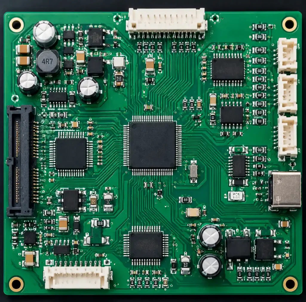
Group functionally related components to shorten net lengths. Placing a processor adjacent to memory chips reduces DDR routing from 80mm to 25mm average, cutting routing demand by 68%. Position decoupling capacitors within 10mm of power pins to minimize loop inductance while consuming less routing area.
Avoid creating routing channels narrower than 3-4 times your minimum trace pitch. Space connectors at board edges with 15-20mm clear area for escape routing. Consider via-in-pad technology for fine-pitch BGAs below 0.8mm pitch—it places filled microvias directly under component pads, eliminating fanout traces and recovering routing channels.
Via Strategy and HDI Considerations
Via strategy directly impacts layer count requirements. Through-hole vias consume routing area on every layer they traverse—a 12mil drill via with 8mil clearance removes 28mil diameter area from routing on every layer it spans.
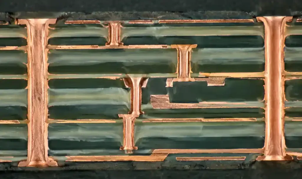
Blind and buried vias reduce this penalty by connecting only necessary layer pairs. A blind via from Layer 1 to Layer 4 consumes routing area only on layers 1-4, leaving remaining layers available. However, blind vias increase manufacturing costs 15-30% compared to through-hole designs.
HDI technology with laser-drilled microvias enables higher routing density that can eliminate 2-4 layers. Microvias with 4mil diameter and 6mil capture pads consume 75% less board area than 12mil through-holes with 24mil pads. For BGA escape routing, microvias allow routing between adjacent balls without dog-bone fanouts. A 1+N+1 HDI stackup reduces layer count by approximately 20% compared to through-hole designs at equivalent routing density.
| Via Type | Diameter (mil) | Capture Pad (mil) | Area per Via (mil²) | Cost Impact |
|---|---|---|---|---|
| Through-hole standard | 12 | 24 | 452 | Baseline |
| Through-hole HDI | 8 | 16 | 201 | +5% |
| Blind via | 10 | 20 | 314 | +15% |
| Microvia (laser) | 4 | 10 | 79 | +20% |
| Stacked microvia | 4 | 10 | 79 | +30% |
Layer Count vs Cost Trade-offs
Manufacturing costs increase exponentially with layer count. A 4-layer board costs $15-25 per square meter in volume production, while 6-layer costs $25-40 (60-80% increase), and 10-layer costs $60-90. Material costs scale linearly, but yield losses and fabrication complexity grow disproportionately.
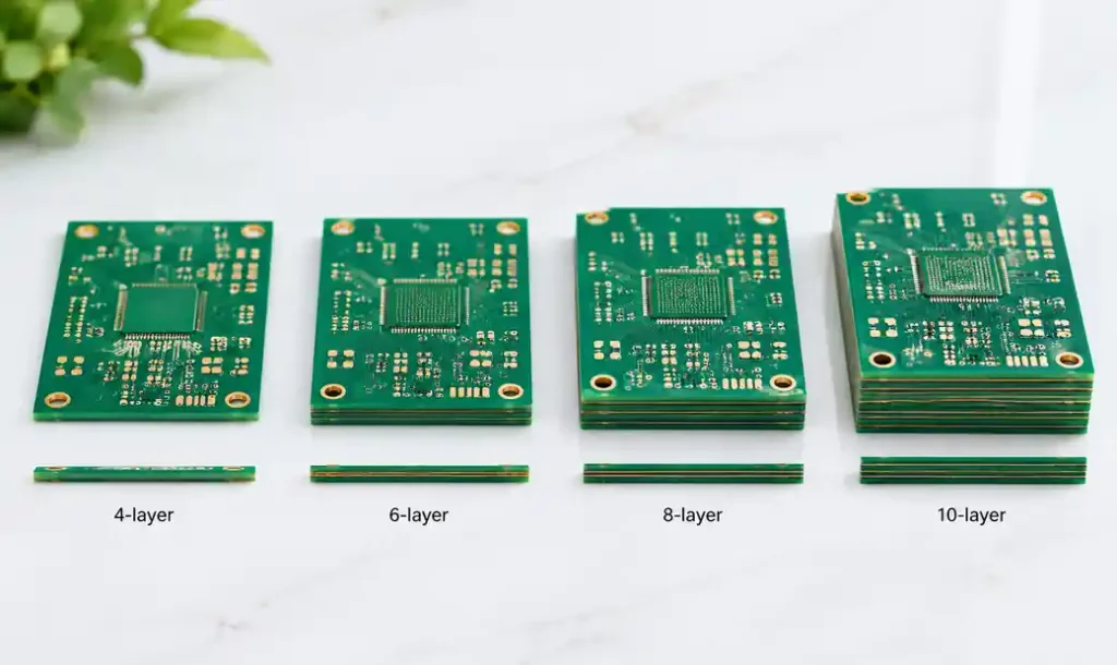
However, reducing layer count through aggressive routing optimization increases design time by 40-60 hours. For volumes below 500 units, engineering time costs exceed the per-board savings from eliminating one layer pair. Above 2,000 units, layer count optimization pays back within first production run.
Assembly costs also factor into decisions. Insufficient layers force component placement on both board sides, requiring double-pass SMT assembly that adds $0.50-1.50 per board. Adding two layers to enable single-sided assembly can reduce total product cost despite higher fabrication expense. Consider increasing board size by 20% instead of adding layers for small form factors—it costs significantly less below 100mm × 100mm.
When to Add Layers vs Redesign
Add layers when routing completion falls below 85% after exhausting placement optimization. Attempting to force remaining 15% of nets creates routing congestion that causes signal integrity problems and complicates future design changes.

Signal integrity requirements may mandate additional layers regardless of routing capacity. High-speed differential pairs above 5 Gbps require adjacent reference planes for controlled impedance and return path integrity. Designs with USB 3.0, PCIe Gen 3+, or 10G Ethernet typically require dedicated signal layers with continuous reference planes.
Power integrity analysis may reveal insufficient plane layers. If PDN impedance exceeds target across 1-100 MHz, adding a power plane pair provides distributed capacitance (1000-2000 pF/in²) that reduces impedance without additional discrete capacitors.
Redesign before adding layers when component placement creates obvious routing bottlenecks. If 50% of routing congestion concentrates in one 20mm × 20mm area, repositioning 3-5 components resolves the issue more effectively than adding layers.
DFM Guidelines for Layer Count Optimization
Specify standard layer counts that manufacturers stock: 4, 6, 8, 10, 12, 16, 20 layers. Odd layer counts (5, 7, 9 layers) require custom fabrication with 15-25% cost premium and extended lead times. Manufacturers pre-stock cores and prepregs for standard counts, enabling faster production and lower costs.
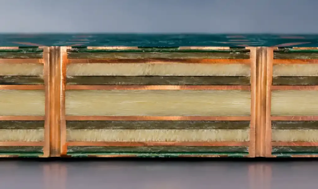
Use symmetric stackups mirroring copper weight and layer structure around the centerline. Asymmetric stackups create thermal expansion mismatch causing board warpage by 5-15mm across 300mm panels during reflow. For 8-layer designs, structure as L1-L2-L3-L4 mirroring L8-L7-L6-L5 with equal prepreg thickness at corresponding positions.
Maintain consistent spacing between signal layers and adjacent reference planes. Varying dielectric thickness from 4mil to 10mil creates impedance discontinuities causing signal reflections above 1 GHz. Specify controlled dielectric thickness (±10% tolerance) for impedance-critical signal layers.
Consult manufacturer capabilities early in stackup planning. Andwin Circuits manufactures PCBs up to 50 layers with controlled impedance and fast delivery in 7-15 days, supporting complex high-density designs with advanced stackup requirements.
Frequently Asked Questions
How do I calculate minimum layer count for my PCB design?
Count total point-to-point connections, estimate average net length, and calculate total routing demand in mm. Divide by per-layer routing capacity (based on trace pitch and usable board area), then apply 40-60% efficiency factor. Add 2-4 dedicated power planes to signal layer count for total layers required.
When should I use HDI technology instead of adding layers?
Use HDI when component pin pitch falls below 0.8mm, routing density exceeds 70% on signal layers, or BGA escape routing consumes more than 3 layers. HDI microvias reduce layer count by 20-30% for high-density designs but increase fabrication costs 20-35% compared to standard through-hole construction.
What is the cost difference between 6-layer and 8-layer PCBs?
Eight-layer PCBs cost 40-60% more than 6-layer in production volumes, approximately $35-45 per square meter vs $25-40 for 6-layer. Cost per board depends on panel utilization—smaller boards fitting more units per panel reduce per-unit costs significantly.
Can I reduce layer count by increasing board size?
Yes, for designs constrained by routing density rather than signal integrity. Increasing board area by 30% provides equivalent routing capacity to adding 2 signal layers but costs 15-25% less in fabrication. However, enclosure constraints and signal path lengths may limit this approach.
How many layers do I need for BGA escape routing?
Divide signal rows across BGA footprint by 2 to get rows requiring breakout, then divide by 2 again for required signal layers. A BGA with 10 signal rows requires approximately 2-3 dedicated layers for escape routing. Fine-pitch BGAs below 0.8mm typically require HDI microvias regardless of layer count.
Conclusion
Layer count optimization balances routing density, signal integrity requirements, power distribution needs, and manufacturing costs. Calculate routing demand early using net count and average length, then apply 50% efficiency factors to determine minimum practical layer count. Strategic component placement, via optimization, and HDI technology reduce layer requirements by 20-40%.
For complex routing challenges requiring advanced stackup design, Andwin Circuits offers high layer count PCB manufacturing up to 50 layers with controlled impedance and fast delivery in 7-15 days. Our DFM engineering team provides stackup optimization consultation to reduce layer count while maintaining signal integrity. Contact us today for layer count analysis and custom PCB manufacturing with competitive factory-direct pricing.