
Antenna PCB Design: PCB Trace Antennas for IoT and Wireless Devices
IoT devices and wireless electronics now exceed 15 billion units worldwide, with over 60% using integrated PCB trace antennas to eliminate external antenna costs and save board space. PCB antenna design directly determines wireless range, power consumption, and FCC/CE certification success—getting the impedance matching and keep-out zones right the first time can reduce product development cycles by 4-6 weeks.
If you want to design reliable PCB antennas for IoT products, then you will need to understand trace antenna types, impedance matching networks, ground plane interactions, and RF layout techniques that separate working prototypes from production-ready wireless devices.
What Are PCB Trace Antennas?
PCB trace antennas are copper traces etched directly onto printed circuit boards that function as radiating elements for wireless communication. These antennas eliminate external antenna components, reducing bill of materials costs and simplifying assembly.
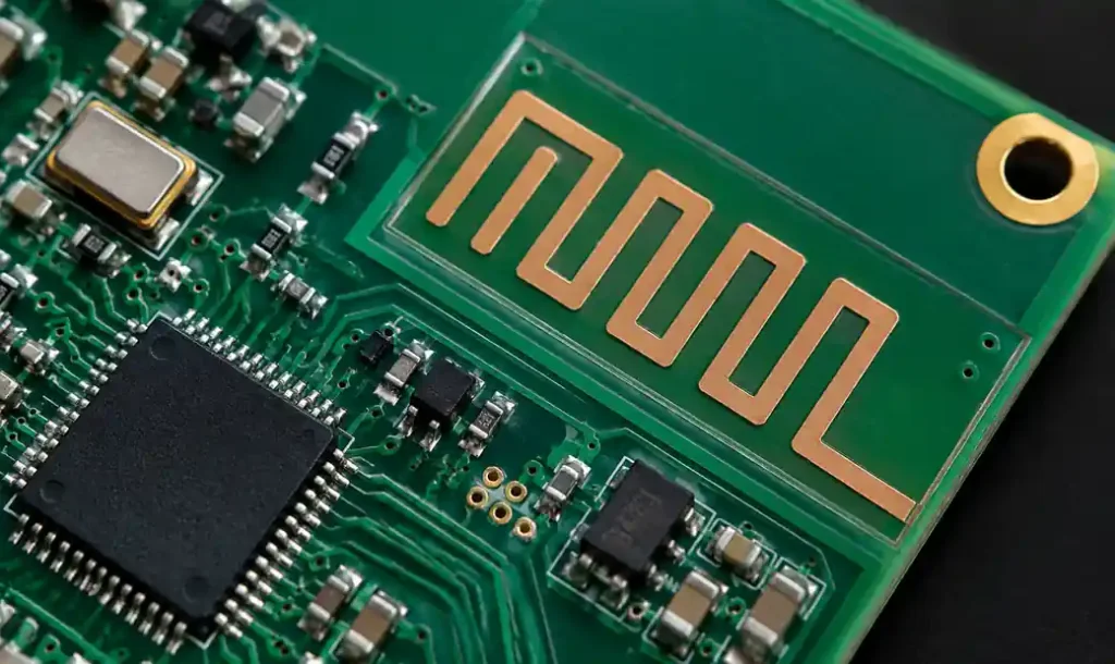
For 2.4 GHz applications like Wi-Fi and Bluetooth Low Energy, typical trace lengths range from 28-32mm (quarter-wavelength adjusted for PCB dielectric constant). The copper trace width, substrate dielectric constant (εr), and board thickness all affect performance.
You can use PCB trace antennas for IoT sensors, wearable devices, smart home products, and any battery-powered application where space and cost constraints make external antennas impractical.
PCB Antenna Types for Wireless Devices
Inverted-F Antenna (IFA)
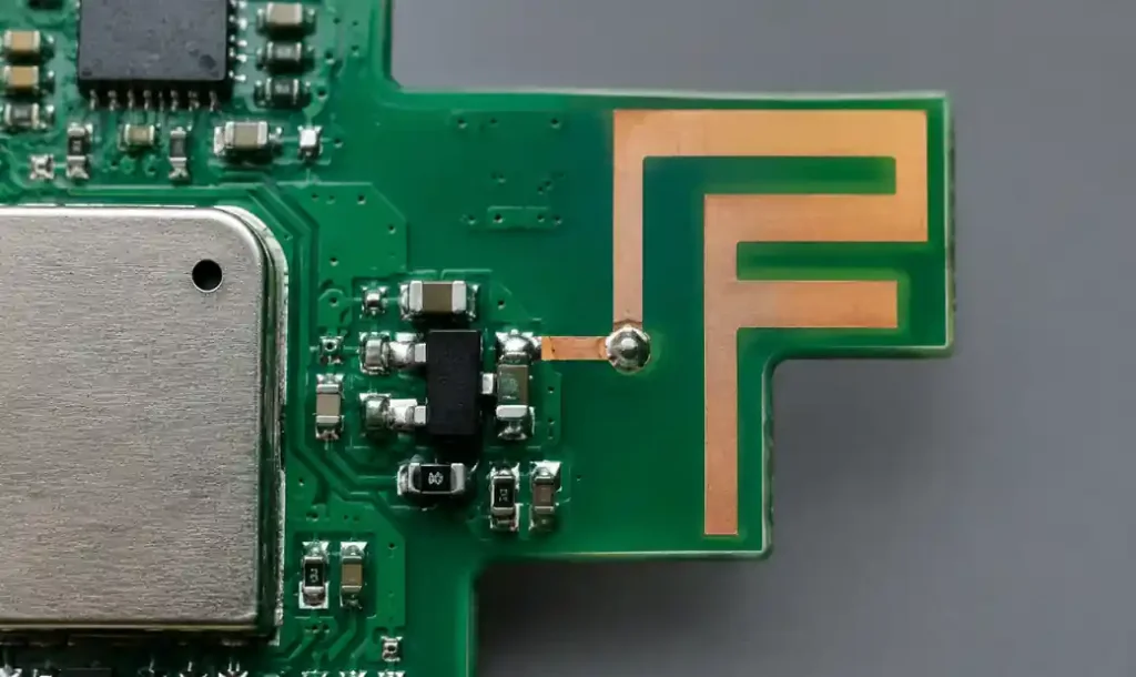
Inverted-F antenna design is the most widely adopted PCB antenna type for 2.4 GHz wireless applications including Wi-Fi, Bluetooth, and Zigbee protocols. The structure consists of a main radiating element with a feed point and a shorting pin to ground, creating the characteristic inverted “F” shape.
The typical IFA for 2.4 GHz measures 25-30mm in length and 7-8mm in width, occupying approximately 200-250mm² of PCB area. This compact footprint provides 2.0-2.5 dBi gain with near-omnidirectional radiation patterns suitable for portable devices.
Monopole and Patch Antennas
Monopole antenna design uses a single straight copper trace extending from the RF feed point. For 2.4 GHz applications, quarter-wave monopoles measure approximately 31mm in length, providing 1.5-2.5 dBi gain with simple layout.
Patch antennas consist of a rectangular copper area separated from a ground plane. These antennas provide higher directivity (4-6 dBi) making them suitable for point-to-point wireless links and directional applications.
| Antenna Type | Typical Size (2.4 GHz) | Gain | Bandwidth | Best Application |
|---|---|---|---|---|
| Inverted-F (IFA) | 25-30mm length | 2.0-2.5 dBi | 5-8% | Wi-Fi, BLE, general IoT |
| Monopole | 31mm length | 1.5-2.5 dBi | 8-12% | Fixed-orientation sensors |
| Patch | 28×38mm area | 4-6 dBi | 3-5% | Directional links, gateways |
Impedance Matching for 50Ω RF Systems
Impedance matching networks ensure maximum power transfer between the RF transceiver (typically 50Ω output) and the PCB antenna, minimizing reflected power and improving wireless range. Poor impedance matching results in high VSWR (Voltage Standing Wave Ratio) above 3:1, which reduces radiated power by 25% or more.
The most common matching network uses an LC configuration with surface-mount capacitors and inductors placed within 3mm of the antenna feed point. Component values are determined through Smith chart analysis or RF simulation software based on the antenna’s measured complex impedance. For a 2.4 GHz IFA antenna measuring 30+j15Ω, typical matching components include a 2.7nH series inductor and 1.5pF shunt capacitor to transform the impedance to 50Ω.
According to IPC-2141 controlled impedance design standards, trace width and spacing must be calculated based on substrate dielectric constant, board thickness, and target impedance. For FR4 substrate (εr ≈ 4.4) with 1.6mm thickness, a 50Ω microstrip trace measures approximately 2.8-3.0mm wide.
Ground Plane Design and Keep-Out Zones
Ground plane configuration fundamentally affects PCB antenna radiation efficiency and resonant frequency. For monopole and inverted-F antenna types, the ground plane acts as the counterpoise element. Inadequate ground plane size reduces radiation efficiency by 40-60% and shifts resonant frequency by 50-150 MHz.
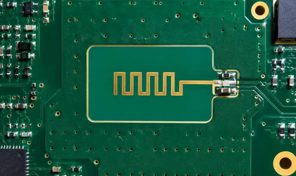
The antenna keep-out zone is a copper-free area surrounding the radiating element where no ground planes, power planes, or signal traces should exist on any PCB layer. This clearance zone typically extends 5-8mm beyond the antenna perimeter for 2.4 GHz designs and 10-15mm for sub-GHz applications.
Ground plane dimensions should extend at least λ/4 (quarter wavelength) in all directions from the antenna feed point. At 2.4 GHz on FR4 substrate, this translates to minimum 30-35mm ground plane extent. You should define keep-out zones in your PCB layout tool as mechanical layers with design rule checks.
PCB Material Selection for RF Performance
PCB substrate material directly affects antenna resonant frequency, bandwidth, and radiation efficiency. Standard FR4 material with εr ≈ 4.4 works well for most 2.4 GHz IoT applications and provides good cost-performance balance.
| Material | Dielectric Constant (εr) | Loss Tangent | Cost | Best Application |
|---|---|---|---|---|
| FR4 Standard | 4.3-4.5 | 0.02 @ 1GHz | 1× | Consumer IoT, BLE devices |
| Rogers RO4003C | 3.38 ±0.05 | 0.0027 @ 10GHz | 4× | Long-range LoRa, outdoor gateways |
Low-loss RF substrates like Rogers RO4003C improve antenna efficiency by 10-15% compared to standard FR4 but increase material costs by 3-5× per board. You should specify low-loss laminates for applications requiring maximum wireless range exceeding 100 meters.
Wi-Fi, BLE, and LoRa Antenna Design Guidelines
2.4 GHz Antenna Design (Wi-Fi and BLE)
Wi-Fi 802.11b/g/n and Bluetooth Low Energy both operate in the 2.4-2.48 GHz ISM band, allowing the same antenna design to serve both protocols. An inverted-F antenna with 30mm radiating element and properly tuned matching network achieves -10 dB return loss across the entire 2.4 GHz band.
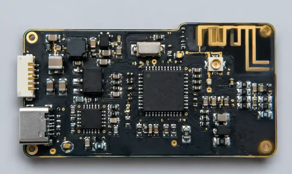
Design the antenna on the top PCB layer at a board edge or corner with 5-7mm keep-out clearance. Use a 50Ω controlled impedance feed line maintaining continuous path from the RF transceiver to the matching network. Place the matching network within 5mm of the antenna feed point using 0402 SMT components.
Sub-GHz LoRa Antenna Design
LoRa protocols (868 MHz EU, 915 MHz US) require significantly larger PCB antennas due to longer wavelengths. A quarter-wave monopole measures approximately 86mm at 868 MHz and 81mm at 915 MHz—dimensions that often exceed available board space in compact IoT nodes.
Meandered monopole designs reduce physical length by 30-40% through serpentine trace patterns. A meandered 915 MHz antenna can fit within 50-60mm length at the cost of 0.5-1.0 dB reduced gain. The ground plane should extend at least 80mm in all directions from the feed point.
Antenna Placement and PCB Layout Best Practices
Antenna placement decisions impact every aspect of wireless performance and must be locked into the mechanical design early. Position the antenna at a PCB edge or corner, as far as possible from high-speed digital circuits, switching power supplies, and LCD displays that generate electromagnetic interference.
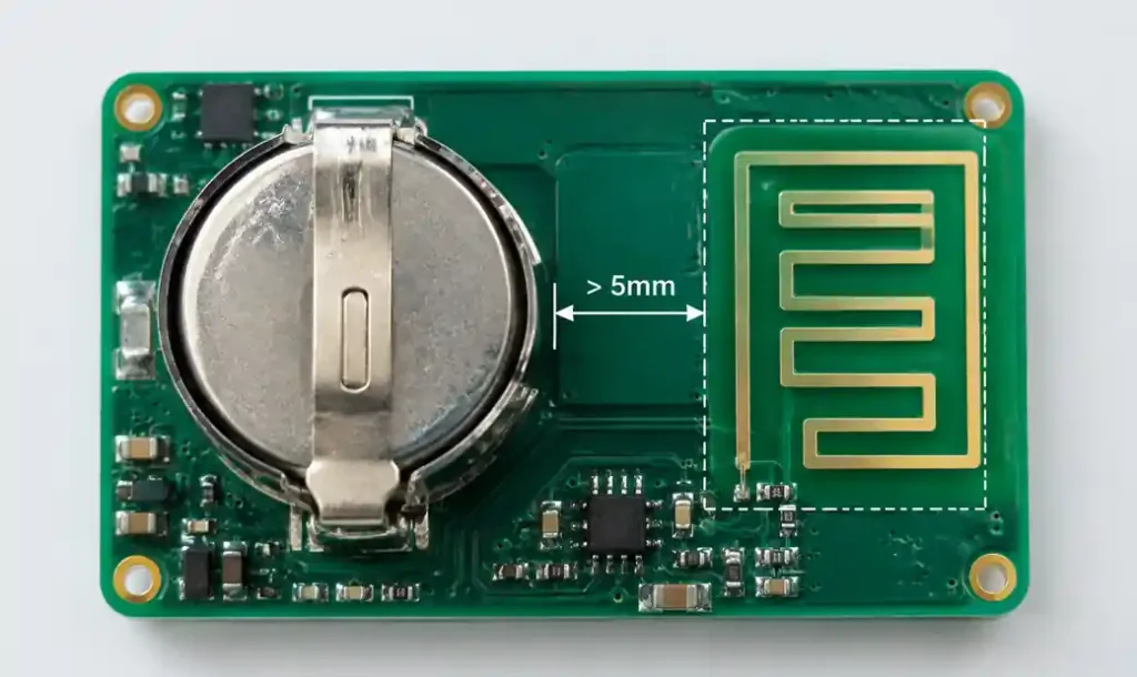
Maintain minimum 15mm separation between the antenna and components that emit EMI, including DC-DC converters and crystal oscillators above 40 MHz. Battery placement significantly affects antenna performance—maintain at least 5mm clearance between lithium cells and the antenna keep-out zone.
Metal enclosures and plastic housings with metallized coatings completely block RF radiation if placed directly over the antenna. Design the product enclosure with a non-conductive window aligned with the antenna location.
Tuning and Testing PCB Antennas
Antenna tuning matches the fabricated PCB antenna to 50Ω system impedance and optimizes resonant frequency. Use a Vector Network Analyzer (VNA) to measure S11 return loss and Smith chart impedance across the frequency range. Target return loss better than -10 dB (-15 dB preferred) at center frequency, which corresponds to VSWR below 2:1.
Radiated performance testing measures antenna gain and radiation pattern per FCC Part 15.247 or EN 300 328 standards. Pre-compliance testing using near-field probes costs $500-2,000 and identifies major antenna problems before formal certification testing at $5,000-15,000 per test configuration.
FCC and CE Certification for Wireless Products
Wireless products using PCB trace antennas must comply with FCC Part 15 (United States), CE RED Directive (European Union), and equivalent regulations before commercial sales. Intentional radiators in the 2.4 GHz ISM band are limited to +30 dBm EIRP (1 watt) for frequency hopping spread spectrum systems.
You should complete pre-compliance testing during prototype development to identify issues before formal certification. Common failure modes include insufficient harmonic suppression, spurious emissions from poorly filtered power supplies, and excessive radiated power on non-hopping channels. Budget 4-8 weeks for certification testing.
Frequently Asked Questions
What is the difference between PCB trace antenna and chip antenna?
PCB trace antennas are copper patterns etched directly onto the circuit board, occupying 200-400mm² of board area with no additional components. Chip antennas are ceramic modules measuring 2×3mm to 5×8mm that mount like SMT components. Trace antennas cost $0 in materials but require RF design expertise and larger board area. Chip antennas add $0.15-0.80 per unit BOM cost but save 60-80% board space.
How do I calculate PCB antenna trace length for 2.4 GHz?
Calculate quarter-wave monopole length using: L = (c / f) × (1 / √εr) × 0.95 / 4, where c = 300,000,000 m/s, f = 2450 MHz, εr = 4.4 for FR4. This yields approximately 30.5mm trace length. For inverted-F antennas, reduce length by 10-15% due to shorting stub effects, resulting in 26-28mm dimensions.
Can I use the same antenna design for Wi-Fi and Bluetooth?
Yes, Wi-Fi 2.4 GHz (2.4-2.48 GHz) and Bluetooth/BLE (2.402-2.480 GHz) operate in the same ISM frequency band. A properly designed 2.4 GHz antenna with adequate bandwidth (minimum 80 MHz) supports both protocols simultaneously.
What causes PCB antenna performance to change after adding an enclosure?
Plastic enclosures add dielectric material (εr typically 2.5-3.5) around the antenna that lowers resonant frequency by 20-80 MHz depending on thickness and proximity. Metal or metallized enclosures block RF radiation entirely if placed over the antenna without a dielectric window. Always tune and test antennas with final production enclosures installed.
How much does poor antenna design reduce wireless range?
Poor impedance matching causing VSWR = 3:1 reduces effective radiated power by 25% (-1.25 dB), cutting range by 15%. Inadequate ground plane can decrease efficiency from 70% to 40% (-2.4 dB loss), reducing range by 25-30%. Combined effects can cause 4-6 dB total system loss, cutting wireless range by 50% or more. Professional controlled impedance PCB design and proper antenna placement are critical.
Conclusion
PCB trace antenna design directly determines IoT product wireless performance, regulatory compliance, and development costs. Proper antenna type selection, accurate impedance matching networks, adequate ground plane sizing, and strict keep-out zone enforcement separate successful wireless products from those requiring expensive board respins.
If you need high-quality PCB manufacturing for IoT and wireless devices, Andwin Circuits offers advanced HDI and flex PCB capabilities with controlled impedance design up to 50 layers. Our RF design verification services include VNA testing and DFM review to ensure your antenna design works correctly before production. Fast turnaround in 7 days for prototypes and 100% quality guarantee help you launch wireless products on schedule.
Contact us today for custom PCB solutions with RF design support, technical specifications, and competitive factory-direct pricing.
Sources: