
Via in Pad PCB Design: When to Use and Manufacturing Considerations
If you work in high-density PCB design, you’ve encountered the routing bottleneck under fine-pitch BGA and QFN packages. Via in pad (VIP) technology places vias directly within component pads, unlocking critical routing channels and improving thermal management—but it introduces manufacturing complexity and cost implications you need to understand.
What is Via in Pad Technology?
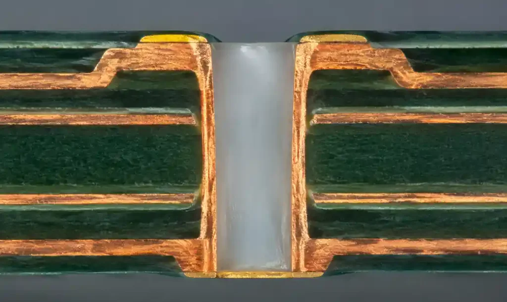
Via in pad places plated vias—through-holes, blind vias, or microvias—directly within surface-mount component pads. Unlike conventional designs routing vias outside the pad area, VIP eliminates fanouts entirely, placing the via hole in the solderable land.
This frees valuable routing space under dense packages and provides direct thermal and electrical paths to inner layers. For BGA packages with 0.8mm pitch or finer, via in pad often becomes the only practical escape routing solution.
According to IPC-4761, proper via treatment is critical because via barrels create pad surface depressions that trap air, moisture, and flux during assembly, leading to solder joint voids.
When to Use Via in Pad
High-Density BGA and QFN Packages
You should consider via in pad for fine-pitch BGA packages where pad spacing leaves insufficient room for traditional via breakouts. Components with 0.8mm pitch or tighter typically require VIP. A 0.5mm pitch BGA has pads approximately 0.25-0.3mm diameter—too small for both solder joint and adjacent via with adequate clearance.
Modern processors, FPGAs, and memory devices routinely use via in pad because routing all signals to perimeter vias would require excessive board area and create signal integrity issues.
Thermal Management Requirements
Power electronics use via in pad for thermal relief. Filled vias under power components create low-resistance thermal paths, reducing junction temperature by 15-20°C versus offset thermal vias.
For LED on aluminum MCPCBs, via in pad with copper-filled microvias provides 2-5 W/mK thermal conductivity—better than the dielectric layer’s 1-3 W/mK.
Signal Integrity Optimization
High-speed digital and RF designs benefit from VIP’s shorter signal paths. Each millimeter adds ~1nH/mm inductance that degrades signal quality. For 10+ Gbps SerDes and 20+ GHz RF circuits, via in pad minimizes stub length and reduces return loss.
Controlled impedance PCBs for 5G infrastructure specify via in pad to maintain signal integrity across layer transitions.
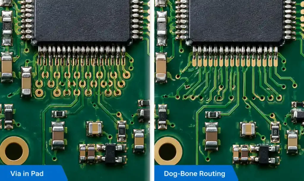
Table 1: Via in Pad vs Traditional Via Escape Comparison
| Parameter | Via in Pad | Traditional Dog-Bone |
|---|---|---|
| Routing Density | Very High | Moderate |
| Board Space Required | Minimal | +15-25% per BGA |
| Thermal Performance | Excellent (direct path) | Good (offset path) |
| Signal Path Length | Shortest | Longer (+2-5mm) |
| Manufacturing Cost | +20-40% | Baseline |
| Assembly Risk | Higher (void formation) | Lower |
| Applications | Fine-pitch BGA, HDI PCB, RF | Standard BGA, general use |
Via in Pad Types and Manufacturing Methods
Unfilled Via in Pad
The basic approach leaves via barrels open after plating. During reflow, molten solder wicks down into the via, reducing joint volume and creating voids. Unfilled VIP is rarely specified for production due to high defect rates.
Resin-Filled and Capped Via in Pad
Industry-standard IPC-4761 Type VII fills vias with non-conductive epoxy resin, then planarizes and caps with copper plating before pad finish. This creates flat, solderable surfaces preventing solder wicking.
The process forces epoxy into via barrels under vacuum, eliminating air pockets. After curing, CNC planarization creates flush surfaces. Final copper electroplating (15-25μm) and ENIG/ENEPIG finish complete the pad.
Resin-filled VIP adds 3-5 days to lead time and increases cost 25-35% versus standard PCB fabrication.
Copper-Filled Via in Pad
High-reliability applications use electroplating to fill via barrels with solid copper, providing 390 W/mK thermal conductivity versus epoxy’s 2 W/mK. This eliminates CTE mismatch in thermal cycling.
Copper filling requires multiple plating cycles, adding 5-7 days and 50-70% cost. Aerospace, military, and automotive applications specify it where performance justifies the premium.

Manufacturing Challenges and Solder Void Prevention
Understanding Solder Void Formation
IPC research shows via depression traps air and flux during stencil printing, creating voids during reflow. Non-filled or poorly filled vias produce 25-40% void levels—exceeding IPC-7095’s 25% limit for non-thermal pads and 15% for thermal pads.
Void mechanisms include outgassing (trapped air expands during reflow), solder wicking (capillary action draws solder into vias), and flux entrapment (volatilized flux generates voids).
Process Control for Void Reduction
Via fill density must exceed 95% to prevent outgassing. Planarization achieves ±25μm flatness. Copper cap thickness of 15-25μm provides pad strength without excessive step height.
Assembly optimization includes extended reflow soak zones, vacuum reflow for critical applications, and stencil apertures 10-15% smaller than pad size to control solder volume.
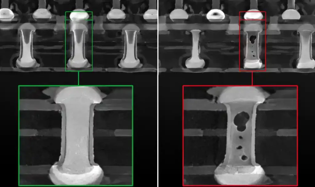
Table 2: Via in Pad Filling Methods Comparison
| Method | Fill Material | Thermal Conductivity | Cost Impact | Lead Time | Best Applications |
|---|---|---|---|---|---|
| Unfilled | None | Poor | Baseline | 0 days | Low-density prototypes only |
| Resin Fill + Cap | Epoxy resin | 2 W/mK | +25-35% | +3-5 days | Standard HDI, BGA escape |
| Copper Fill | Electroplated Cu | 390 W/mK | +50-70% | +5-7 days | High power, aerospace |
| Conductive Paste | Silver/copper paste | 20-50 W/mK | +35-45% | +4-6 days | Moderate thermal needs |
Design Rules and IPC-4761 Guidelines
Via Diameter and Pad Sizing
Via finished hole diameter should not exceed 60% of pad diameter. A 0.3mm pad accommodates maximum 0.15-0.18mm finished via. Laser-drilled microvias of 0.1-0.15mm work well.
Annular ring on inner layers must meet IPC-6012 Class 3 minimum 50μm (2mil) after registration tolerances. HDI with sequential lamination allows smaller capture pads.
Via Depth and Layer Span
Blind microvias spanning 1-2 layers minimize fill volume and void risk versus through-holes. For 1.6mm boards, through-holes require 2x the fill volume of L1-to-L2 blind vias.
Stacked microvias—multiple blind vias aligned vertically—provide the most reliable VIP for 8+ layer HDI. Each segment is individually filled during its build-up sequence.
Current Handling Capacity
A standard 0.15mm diameter through-hole via with 25μm barrel plating handles 0.5-0.8A continuous per IPC-2152. Copper-filled vias support 2-3A due to solid copper cross-section.
For power delivery, use copper-filled VIP or via arrays—multiple filled vias per pad.
Cost Analysis and ROI
Via in pad costs 25-40% more than standard PCBs but delivers ROI through 15-25% board size reduction, potential 2-layer elimination, better yields from improved thermal management, and competitive necessity for fine-pitch components.
Fabrication cost factors include via filling (+15%), planarization (+10%), extended plating (+8%), and inspection (+5%). High-volume orders (500+ panels) reduce per-unit cost 10-15%.
Applications Across Industries
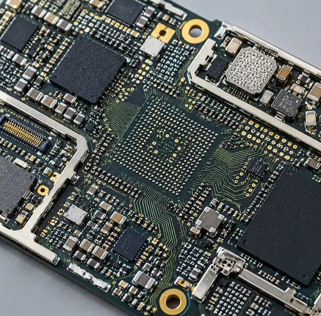
Smartphones use 500-800 VIP locations with resin-filled blind microvias on 8-12 layer HDI. Automotive ADAS specifies VIP for radar processors meeting AEC-Q100’s 1000 thermal cycles. Medical devices and aerospace require copper-filled VIP with 100% X-ray verification. Industrial IoT uses silicone-modified epoxy fills for -40°C to +85°C operation.
Frequently Asked Questions
Q: Can I use via in pad for prototypes?
A: Yes, expect 7-10 day lead times and 40-50% cost premium. Consider dog-bone fanouts for initial builds, transition to VIP for production optimization.
Q: What surface finish works best?
A: ENIG provides flattest surface and best solderability. ENEPIG adds wire bonding capability. Avoid HASL due to uneven coating.
Q: Thermal cycle reliability?
A: Quality resin-filled VIP exceeds 500 cycles for consumer and 1000+ for automotive per IPC-4761 Type VII. Copper-filled achieves 2000+ cycles.
Q: Via in pad for all BGA pads?
A: Specify only where needed—inner ball rows and thermal pads. Perimeter balls often route without VIP, reducing cost.
Q: What minimum pitch requires it?
A: Most transition at 0.8mm pitch. Some route 1.0mm with micro-vias in breakouts, but 0.65mm and finer universally require VIP.
Conclusion
Via in pad solves critical routing and thermal challenges in high-density PCBs. Resin-filled and copper-capped vias per IPC-4761 Type VII provide reliable BGA and QFN assembly when you need maximum density and thermal performance.
The 25-35% cost increase and 3-5 day lead time addition offset by board size reduction and improved performance. For fine-pitch components, VIP is often the only option. Proper design rules, fill process control, and assembly optimization minimize voids and maximize yield.
When specifying VIP, work with experienced HDI manufacturers providing process capability data and thermal cycling qualification. Andwin Circuits offers up to 50-layer capability, 7-day turnaround, and IPC Class 3 quality with IATF 16949 certification for automotive, medical, and telecommunications applications.
Contact our engineering team for via in pad design review and detailed capability specifications.