
Back Drilling in PCB: Stub Removal for High-Speed Design
Signal integrity failures in high-speed PCB designs often trace back to overlooked via stubs. When your 25 Gbps SerDes interface fails eye margin testing or DDR5 signals show unexplained jitter above 10 ps, the culprit is typically a via stub creating resonance within your operating bandwidth. Back drilling solves this by mechanically removing unused copper barrel sections, pushing stub resonant frequency beyond critical signal harmonics and recovering precious insertion loss margin for multi-gigabit links.
What Are Via Stubs and Why They Matter
A via stub is the unused plated copper barrel extending beyond the last connected signal layer. In a 14-layer board where signal transitions from Layer 1 to Layer 6, the copper section from Layer 7 through Layer 14 serves zero electrical function yet acts as an unterminated transmission line stub reflecting energy back into your signal path.
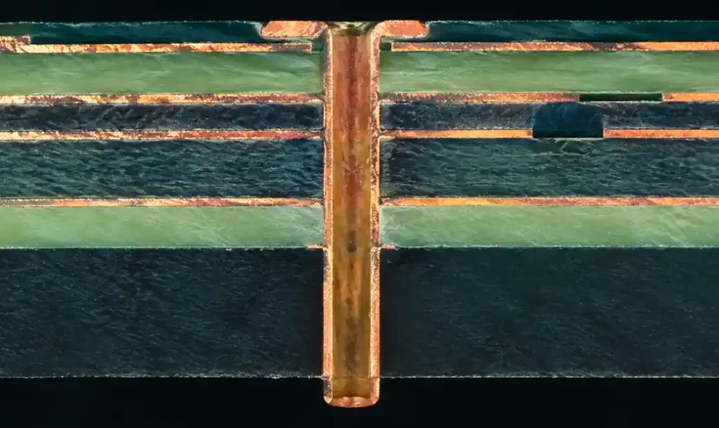
This stub behaves as a quarter-wave resonator. At the frequency where stub electrical length equals λ/4, reflected signal returns 180° out of phase, creating deep notches in insertion loss. For a 45-mil stub in FR4, first resonance appears near 8.3 GHz with additional nulls at each odd harmonic.
Measurements show via stubs cause 1.5-3.5 dB insertion loss degradation at frequencies above 5 GHz. When your signal harmonics land near stub resonance, you see eye closure, jitter amplification, and bit error rates that equalization cannot fully recover.
The Back Drilling Process Explained
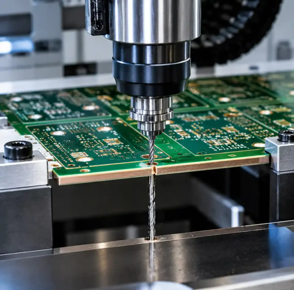
Back drilling—also called controlled depth drilling—uses a slightly larger drill bit (typically 8-14 mils larger) entering from the board’s opposite side after initial drilling and plating. The operation removes plated copper, stopping 5-12 mils (commonly 8-10 mils) before reaching the target pad.
| Back Drilling Parameter | Typical Value | Tight Control | Standard Reference |
|---|---|---|---|
| Back Drill Bit Oversize | 8-12 mils larger | 10 mils | IPC-6012 Class 3 |
| Target Residual Stub | 8-10 mils | 6-8 mils | Per design |
| Depth Control Tolerance | ±5 mils | ±3 mils | Manufacturing capability |
| Registration Accuracy | ±4 mils | ±2 mils | IPC-6012 Class 2/3 |
| Maximum Aspect Ratio | 10:1 | 8:1 | Mechanical limits |
Registration accuracy between original and back drill must stay within ±3 mils, requiring optical alignment and proper fixturing. Process tolerance of ±5 mils means 8-mil target yields 3-13 mil actual range across panels.
When Back Drilling Becomes Necessary
The decision to implement back drilling depends on signal frequency, data rate, and insertion loss budget.
| Interface Type | Data Rate | Nyquist Frequency | Stub Length Threshold | Back Drilling Required |
|---|---|---|---|---|
| PCIe Gen 3 | 8 GT/s | 4 GHz | >50 mils | Consider for >12 layers |
| PCIe Gen 4 | 16 GT/s | 8 GHz | >30 mils | Yes for >8 layers |
| PCIe Gen 5 | 32 GT/s | 16 GHz | >15 mils | Mandatory for all signal vias |
| USB 3.2 Gen 2 | 10 Gbps | 5 GHz | >35 mils | Yes for >10 layers |
| 25G Ethernet | 25.78125 Gbps | 12.9 GHz | >18 mils | Yes for all transitions |
| 100G (4×25G) | 25.78125 Gbps per lane | 12.9 GHz | >15 mils | Mandatory |
| DDR5-4800 | 4.8 GT/s | 2.4 GHz | >60 mils | Consider for dense designs |
| DDR5-6400 | 6.4 GT/s | 3.2 GHz | >45 mils | Yes for >10 layers |
PCIe Gen 3 at 8 GT/s sometimes avoids back drilling in 8-10 layer boards with careful via placement. PCIe Gen 4 at 16 GT/s demands back drilling for transitions in boards exceeding 8 layers. PCIe Gen 5 at 32 GT/s requires back drilling on virtually all signal vias plus residual stub control under 6 mils.
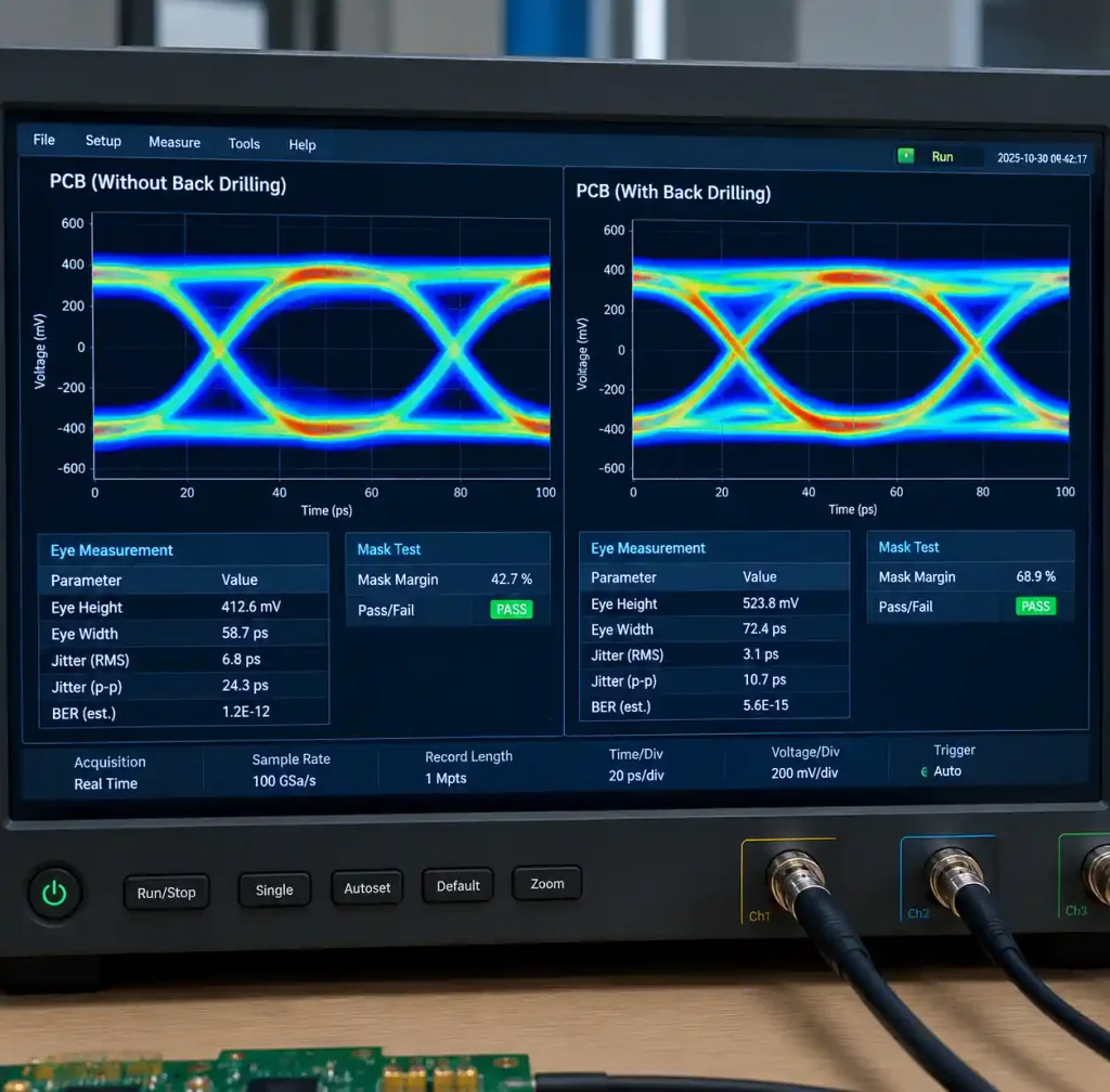
Modern protocols specify maximum insertion loss: PCIe Gen 5 allows -28 dB. A 40-mil via stub consumes 2-3 dB at 16 GHz, making back drilling mandatory for compliance.
Cost Analysis and Economic Trade-offs
Back drilling adds 15-30% to PCB fabrication cost depending on complexity, via count, and manufacturer capability. For a 12-layer prototype with 180 signal vias requiring back drilling, expect $350-750 additional cost. Production volumes above 150 panels see premium drop to 12-18%.
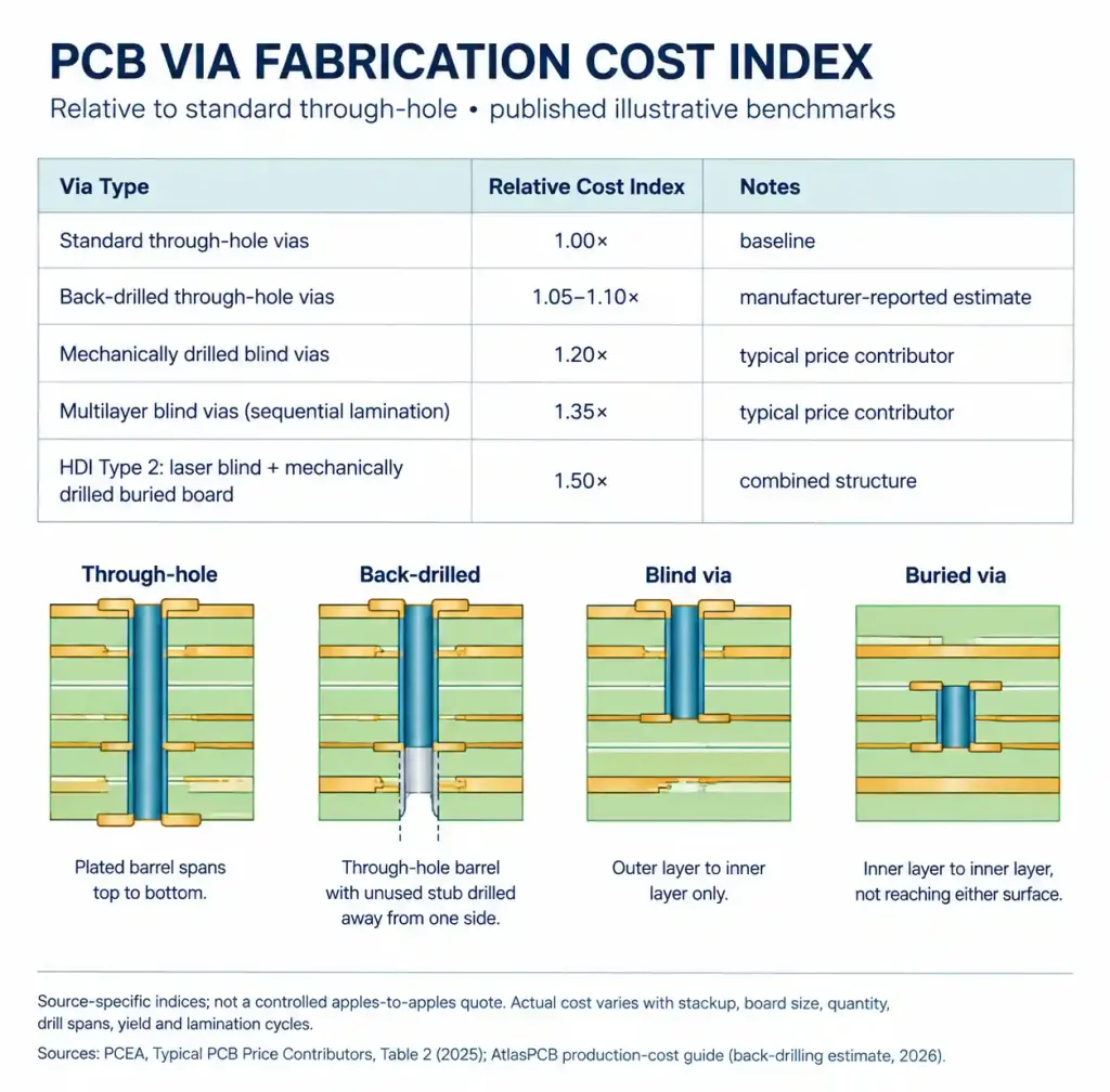
Standard through-hole vias cost 1.0× baseline, back-drilled PTH runs 1.15-1.30×, blind vias jump to 1.8-2.5×, and buried vias reach 2.0-3.0× due to sequential lamination.
Back drilling delivers optimal cost-performance when you need through-hole reliability but must eliminate stub resonance. It avoids expensive sequential build-up required for blind and buried via while providing comparable electrical performance for 10-56 Gbps links.
Design Rules for Manufacturing Success
Successful back drilling requires design rules accounting for manufacturing tolerances.
Minimum stub length: 25 mils. Shorter stubs cannot be reliably back drilled due to registration tolerance.
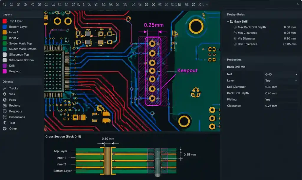
Target residual stub: 8-10 mils balances yield and performance. Specifications under 6 mils require advanced control and increase cost 20-35%.
Pad size adjustment: Add 8-12 mils to standard pad diameter on termination layer, providing margin for registration error.
Layer transition strategy: Design routing to transition at layers where resulting stub after back drilling remains under 10 mils.
Aspect ratio limits: Back drilling depth cannot exceed 10:1 (depth:drill diameter). For 28-mil back drill bit, maximum depth is 280 mils.
Keep-out zones: Maintain 20-25 mil clearance between back-drilled vias and adjacent features to prevent damage.
Alternative Stub Mitigation Strategies
When back drilling proves impractical, consider these alternatives.
Blind vias: Stop on internal layers without penetrating entire board. A blind via from Layer 1 to Layer 6 has zero stub beyond Layer 6. Cost runs 1.8-2.5× standard drilling, requires sequential lamination.
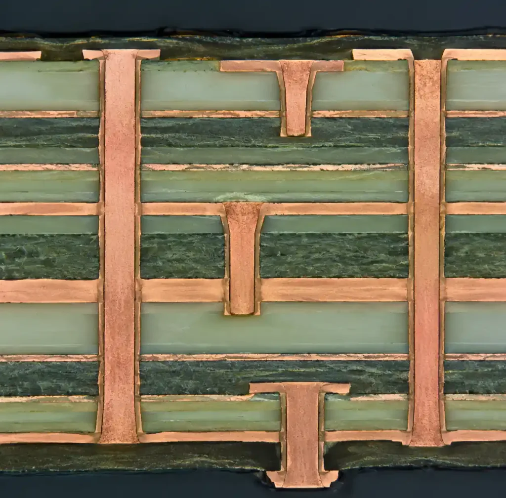
Via-in-pad: Places via under BGA pad, then fills with epoxy and caps with copper. Eliminates stub effects but requires plugging adding $120-280 per panel. Via-in-pad needs careful planarization.
Offset via transitions: Route signal to via positioned for short natural stub length. Costs nothing but restricts routing flexibility.
Microvia technology: Use laser-drilled microvias spanning 1-2 layers for stub-free transitions. Requires HDI build-up, increasing cost 80-150% versus back drilling.
Manufacturing Verification and Testing
Manufacturers verify back drilling using multiple techniques per IPC-6012 qualification requirements.

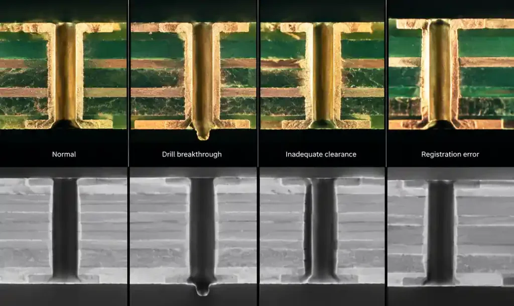
X-ray cross-section: Destructive testing on sample coupons confirms residual stub length, checks for drill breakthrough, and verifies copper barrel integrity within ±5 mil tolerance.
Time-domain reflectometry (TDR): Non-destructive electrical verification. Successful back drilling removes secondary reflection, leaving only via barrel impedance change visible.
C-SAM acoustic microscopy: Detects delamination around back-drilled vias from mechanical stress. Critical for Class 3 applications per IPC-6012 standards.
Microsection analysis: Cross-section examination verifies barrel plating quality, absence of smear, and proper clearance from target pad.
For qualification, manufacturers cross-section minimum 3 coupons per panel, measuring residual stub to ±0.5 mil accuracy with Cpk > 1.33.
Integration with Signal Integrity Design
Back drilling integrates with other signal integrity techniques to meet link insertion loss budgets.
Combine back drilling with controlled impedance design maintaining 50Ω single-ended or 100Ω differential through via transitions. Via barrel impedance typically drops to 35-45Ω; adjust antipad size to minimize return loss.
For 25-56 Gbps PAM4 signaling, back drilling requires proper via antipad optimization. Via capacitance must stay below 0.4 pF for <1 dB insertion loss at 28 GHz. Use antipad diameter 3-4× via barrel diameter.
Stack back-drilled vias vertically when routing requires layer transitions exceeding single via capability, commonly used in high-layer-count boards above 24 layers.
Specify back drilling during PCB design-for-manufacturing review, not after layout completion.
Common Pitfalls and How to Avoid Them
Several mistakes compromise back drilling effectiveness.
Insufficient residual stub margin: Specifying 5-mil residual with ±5 mil tolerance risks drill breakthrough. Maintain minimum 8-mil target.
Inadequate keepout: Back drill can damage nearby features if clearance insufficient. Enforce 20-mil minimum keepout radius.
Missing fabrication notes: Gerber files must explicitly identify back-drilled vias with target depth and tolerance. Provide fabrication drawing showing cross-section with dimensions.
Wrong via drill size: Using minimum drill size increases aspect ratio, making depth control harder. For boards >120 mils thick, specify minimum 12-mil original via diameter.
FAQ
Q: What is the typical cost increase for back drilling?
Back drilling adds 15-30% to PCB fabrication cost for prototypes, dropping to 12-18% for production volumes above 150 panels. A 12-layer prototype might see $350-750 additional cost for 180 back-drilled vias.
Q: Can all PCB manufacturers perform back drilling?
No. Back drilling requires CNC equipment with precision depth control and IPC-6012 qualification. Verify manufacturer capability before committing designs.
Q: How do I know if my design needs back drilling?
If first resonance or odd harmonics fall within your signal bandwidth, back drilling is necessary. For PCIe Gen 4 and faster, back drill all signal vias in boards exceeding 8 layers.
Q: What’s the difference between back drilling and blind vias?
Back drilling mechanically removes copper from plated through-hole, while blind vias never penetrate entire board. Back drilling costs 15-30% more than standard PTH; blind vias cost 80-150% more.
Q: Can via-in-pad replace back drilling?
Via-in-pad eliminates stubs but requires epoxy filling adding $120-280 per panel. Use via-in-pad for BGA fanout; use back drilling for signal layer transitions.
Q: What is residual stub after back drilling?
Residual stub is remaining copper barrel between back drill termination and target pad, typically 8-10 mils with ±5 mil tolerance.
Q: Does back drilling affect board reliability?
Properly executed back drilling per IPC-6012 Class 3 does not compromise reliability when registration accuracy stays within ±3 mils.
Q: What layer count requires back drilling?
No fixed threshold; decision depends on signal frequency and board thickness. PCIe Gen 5 requires back drilling even in 6-layer boards for via stubs exceeding 15 mils.
Conclusion
Back drilling provides proven, cost-effective solution for via stub removal in high-speed PCB designs operating above 5 GHz. The 15-30% cost increase delivers measurable signal integrity improvement, pushing stub resonance beyond critical harmonics and recovering 1.5-3.5 dB insertion loss margin essential for multi-gigabit links. Proper implementation requires coordination between designer and manufacturer during DFM review, specifying residual stub targets, registration tolerances, and verification methods.
If you need high-quality PCB manufacturing with back drilling capabilities for your high-speed design, Andwin Circuits offers advanced controlled depth drilling with 8-mil residual stub control and ±3 mil registration accuracy for boards up to 50 layers. Our facility is certified to ISO 9001, IATF 16949, and UL standards with fast delivery in 7-15 days.
Contact us today for custom PCB solutions with back drilling, technical specifications, DFM support, and competitive factory-direct pricing.