
PCB Fiducial Marks: Placement Rules for Automated Assembly
Place three fiducial marks in non-collinear triangular arrangement at minimum 50mm spacing with 1mm copper diameter and 2mm solder mask clearance to achieve ±0.025mm placement accuracy for fine-pitch BGAs and 01005 components. IPC-7351B requires global fiducials on every board undergoing automated assembly because improper fiducial design causes 15-25% of component placement errors and solder joint defects in high-volume SMT production.
If you design PCBs for automated assembly, then proper fiducial mark placement directly affects yield, reduces rework costs, and prevents field failures. These small copper reference points enable pick-and-place machines, stencil printers, and AOI systems to compensate for board warpage, thermal expansion, and manufacturing tolerances—achieving micron-level accuracy even when your board arrived at the assembly line rotated or shifted by several millimeters.
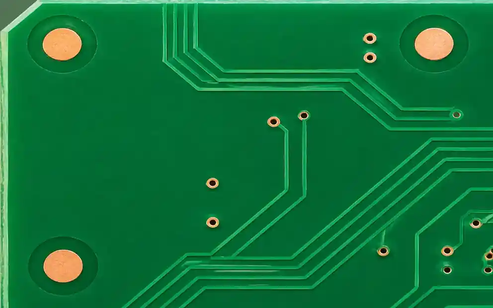
What Are PCB Fiducial Marks?
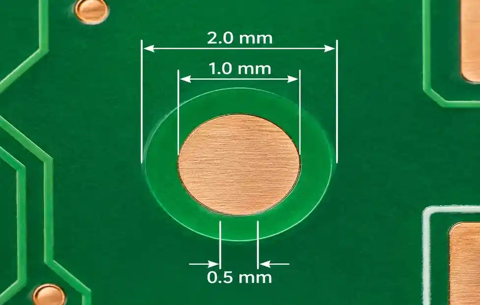
PCB fiducial marks are precision optical reference points—typically 1mm diameter bare copper circles surrounded by 2mm minimum solder mask clearance—that machine vision systems use to establish accurate X-Y coordinates and rotation angle before placing components. The term “fiducial” derives from the Latin word for “trust” because assembly equipment trusts these marks as the definitive positional reference for every operation.
According to IPC-7351B standards, fiducials must provide sufficient optical contrast between copper and solder mask. The standard implementation uses exposed copper without solder mask coverage in the center, surrounded by a keep-out zone free of silkscreen, traces, or other features that could confuse vision algorithms.
You can specify fiducial marks for global board-level alignment, local alignment near fine-pitch components (BGAs, QFNs, 0201/01005 passives), and panel-level alignment when multiple boards populate a production panel. Each fiducial type serves distinct purposes in the assembly process.
Types of Fiducial Marks and When to Use Each
| Fiducial Type | Quantity | Location | Purpose | When Required |
|---|---|---|---|---|
| Global Board Fiducials | 3 minimum | Diagonally opposite corners + third non-collinear | Board-level X-Y-θ alignment | Every assembled board |
| Local Component Fiducials | 2-3 per component | Within 5mm of package outline | Fine-pitch alignment | BGA ≤0.5mm pitch, QFN, 01005 |
| Panel Fiducials | 3 minimum | Panel corners outside V-score | Panel registration | Multi-board production panels |
| Stencil Fiducials | 3 matching board | Corners for triangulation | Paste print alignment | All boards using stencils |
Global Board Fiducials: Three-Point Triangulation
Global fiducials correct X-axis offset, Y-axis offset, and rotational error (theta) for the entire board. Two fiducials establish X-Y position and rotation, but the third fiducial is critical—it enables scaling compensation to detect FR-4 material expansion or contraction from moisture absorption and thermal cycling.
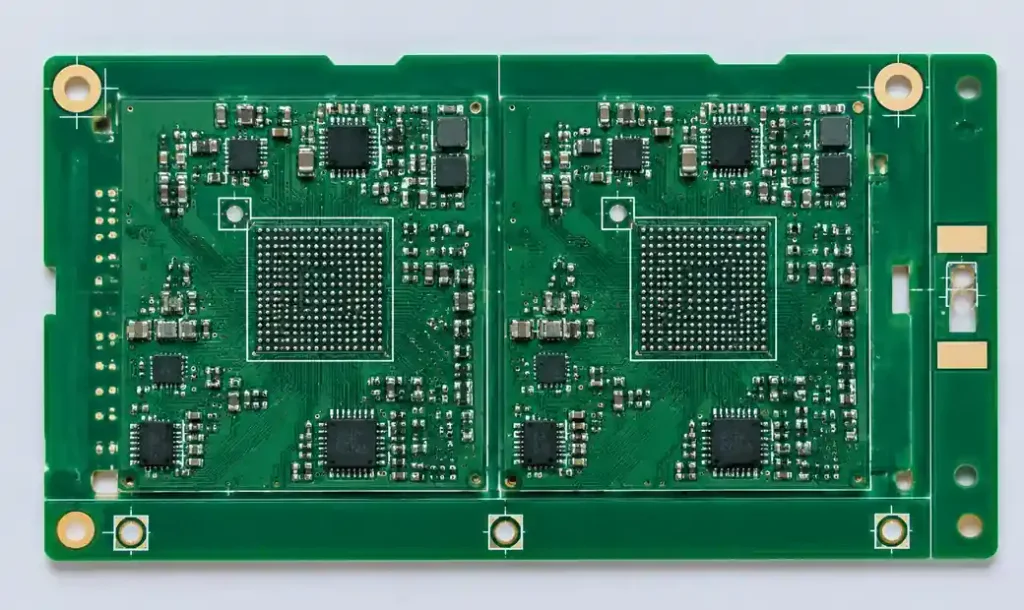
The physics of three-point alignment: Pick-and-place machines calculate a transformation matrix from your CAD coordinates to actual board position. Two points define translation and rotation (4 degrees of freedom), while the third point adds scaling and non-orthogonal correction (2 additional degrees). Without this third point, a board stretched 0.2% from humidity creates systematic placement errors across its entire area.
Place global fiducials at maximum diagonal separation. On a 100mm × 150mm board, corner fiducials separated by the full 180mm diagonal distance deliver 3× better rotational accuracy than edge placement at 100mm separation. For rectangular boards, position two fiducials at opposite corners and the third offset from the diagonal centerline by at least 20mm to avoid collinearity.
Local Component Fiducials: When Global Alignment Isn’t Enough
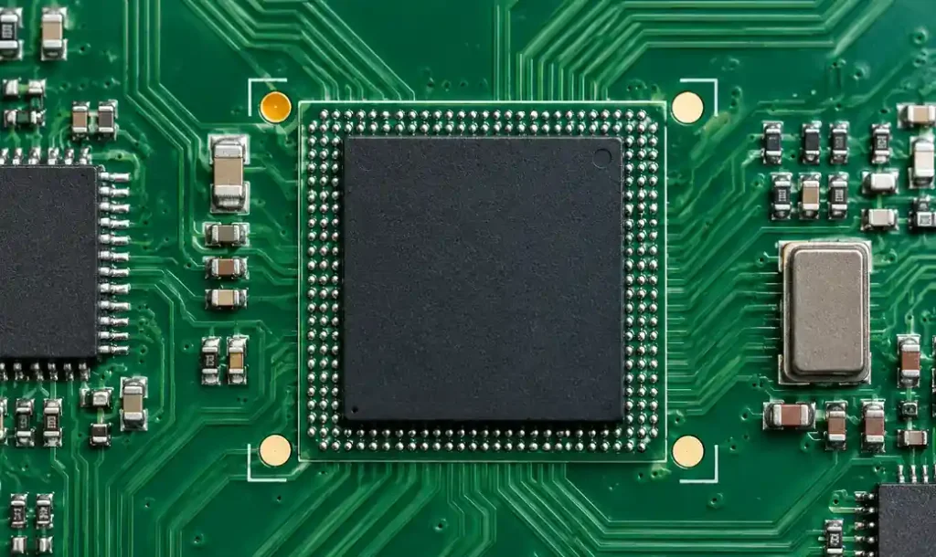
Fine-pitch components with pitch ≤0.5mm (0.4mm BGAs, QFN packages, 01005 passives) require local fiducials within 5mm of the package outline. Global board fiducials compensate for board-level distortion, but localized warpage, copper pattern stress, and laminate inconsistencies create positional errors at component scale.
Testing data from production lines shows that 0.4mm pitch BGAs placed using only global fiducials exhibit 0.08-0.12mm placement variation—exceeding the ±0.05mm tolerance required for reliable solder joint formation. Adding local fiducials reduces this to 0.02-0.03mm variation by referencing features immediately adjacent to the landing pattern.
Place two local fiducials diagonally across the component package at minimum 10mm separation. The fiducials must reside on the same PCB layer as the component pads—do not place local fiducials on the opposite side of the board, as the vision system cannot compensate for board thickness and internal layer misregistration.
IPC-7351B Fiducial Design Standards
Physical Specifications: Size, Clearance, and Contrast
IPC-7351B specifies fiducial diameter based on camera resolution and field of view. The industry standard: 1mm diameter copper pad with 2mm diameter solder mask opening, creating a 0.5mm annular ring of exposed solder mask around the copper. This 2:1 ratio provides optimal optical contrast for machine vision edge detection algorithms.
For compact designs where 1mm fiducials consume excessive board real estate, you can use 0.5mm fiducials with 1mm solder mask clearance, maintaining the 2:1 ratio. However, camera systems require higher resolution and better lighting to reliably detect smaller fiducials, potentially increasing equipment cost and reducing throughput.
The copper pad must be bare—no solder mask coverage, no surface finish coating in the center region. ENIG, HASL, or OSP finishes on fiducial copper create irregular reflectivity that degrades vision system performance. Most PCB fabricators automatically leave fiducials bare copper unless you explicitly specify otherwise in fabrication notes.
Clearance requirements extend beyond solder mask: maintain 3mm minimum keep-out zone free of silkscreen text, logo graphics, copper traces, and component bodies. Vision algorithms detect fiducial edges by analyzing brightness gradients, and features within this zone create false edges that reduce position accuracy by 0.05-0.15mm.
Fiducial Placement Rules for Maximum Assembly Accuracy
Rule 1: Diagonal Separation and Non-Collinear Triangle
Position three global fiducials forming a triangle with maximum area relative to board size. The optimal configuration places two fiducials at opposite corners (maximum diagonal separation) and the third at 90° offset from the diagonal centerline.
Why diagonal matters: Rotational accuracy scales linearly with fiducial separation distance. A 0.01° rotation error over 50mm spacing creates 0.009mm lateral displacement, while the same error over 150mm spacing creates 0.026mm displacement—making the rotational error 3× more detectable and correctable.
Collinear fiducials (three points on a straight line) eliminate the machine’s ability to detect rotation errors perpendicular to that line. Production data shows collinear fiducial placement increases theta correction failure rate from <0.1% to 8-12%, particularly on flex PCBs and thin boards prone to twisting.
Rule 2: Edge Clearance and Mechanical Reference
Maintain 5mm minimum distance from fiducial center to board edge or V-score line. This clearance prevents fiducial damage during depaneling, routing, or handling, and ensures the fiducial remains visible when boards rest in assembly fixtures.
For V-scored panels, place fiducials on the actual board area, not in the panel rails. Panel rail fiducials become inaccessible after depaneling, forcing assemblers to use less accurate visual alignment or to add extra fiducials in prime board real estate.
Position fiducials outside component keepout zones but avoid placement in connector overhang regions. When connectors extend beyond the board edge (HDMI, USB-C, card edge connectors), fiducials in these zones become obscured during assembly, forcing machines to abort or proceed with reduced accuracy.
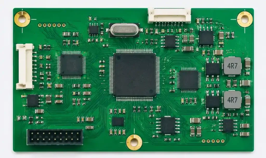
Rule 3: Asymmetric Placement Prevents Orientation Errors
Design fiducial patterns that are asymmetric in both X and Y axes. This prevents 180° rotation errors when boards load incorrectly into assembly fixtures. Symmetric fiducial placement (such as four fiducials at board corners) allows machines to establish valid transformation matrices even when boards rotate 180°, leading to components placed on wrong surfaces or oriented incorrectly.
The fool-proof pattern: place two fiducials along one long edge at 1/4 and 3/4 positions, and one fiducial on the opposite edge at 1/2 position. This triangle configuration is impossible to match after 180° rotation, forcing the vision system to flag orientation errors rather than proceeding with incorrect alignment.
Common Fiducial Placement Mistakes That Cause Assembly Failures
Mistake 1: Fiducials Too Close Together
Placing fiducials at <50mm separation, particularly on boards >100mm in any dimension, reduces rotational error detection by 40-60%. Short baseline separation makes small angular errors indistinguishable from placement noise, leading machines to apply incorrect rotation corrections that compound across the assembly.
Real production example: A 150mm × 200mm board with three fiducials clustered within a 60mm corner area experienced 0.15° systematic rotation error that went uncorrected. This translated to 0.5mm lateral displacement at component locations 200mm from fiducial centroid, causing 100% failure rate for 0.4mm pitch BGA assembly until fiducials relocated to corners.
Mistake 2: Fiducials in Copper Pour or Ground Plane
Placing fiducials within solid copper pour areas creates thermal imbalance during reflow. The large copper mass conducts heat differently than isolated fiducial pads, causing localized warpage that shifts the fiducial position by 0.05-0.10mm relative to components. This thermal distortion remains invisible to room-temperature vision systems but manifests during 245°C reflow peak temperature.
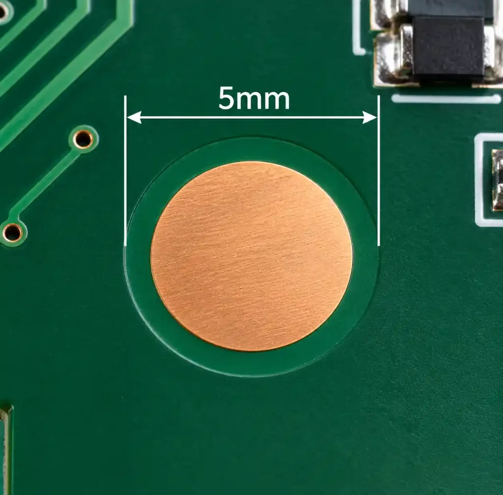
Solution: create 5mm diameter copper relief in ground planes surrounding each fiducial. This thermal isolation ensures fiducial copper and component pad copper experience identical reflow profiles and thermal expansion behavior.
Mistake 3: Rail Fiducials for Fine-Pitch Components
Panel rail fiducials work adequately for standard 0.5mm pitch components but fail for fine-pitch designs because panel distortion (bowing, twist, edge warp) increases with distance from the actual board. A component 80mm from rail-mounted fiducials experiences 2-3× the positional error compared to using on-board fiducials 40mm away.
The physics: Panel rails exist outside the structural core of the board laminate. Pressure variations during lamination create differential stress between board and rail regions, manifesting as 0.05-0.15mm positional offset that varies board-to-board within the same panel. This board-to-board variation makes statistical process control impossible.
Specify board-level fiducials that remain with the PCB after depaneling for any assembly containing components with ≤0.5mm pitch. This requirement applies to HDI PCB designs, BGA assemblies, and miniaturized consumer electronics where placement accuracy directly affects yield.
Fiducial Requirements for Different Assembly Technologies
| Assembly Type | Fiducial Requirement | Placement Accuracy Needed | Fiducial Spacing |
|---|---|---|---|
| Standard SMT (0603, 0402) | 3 global | ±0.10mm | ≥50mm |
| Fine Pitch (0201, 01005) | 3 global + local per zone | ±0.05mm | ≥80mm global, 10-15mm local |
| BGA ≤0.5mm pitch | 3 global + 2-3 local per BGA | ±0.025mm | ≥100mm global, 8-12mm local |
| Flex PCB | 4-5 global (flex distortion) | ±0.08mm | Maximum diagonal |
| Panel Assembly | 3 panel + 3 per board | ±0.10mm | Panel corners + board corners |
Stencil Printing Fiducials
Stencil printers use fiducials to align the stencil apertures with PCB pads before printing solder paste. Printing alignment directly affects paste volume, which determines 70-80% of solder joint quality and up to 60% of assembly defects according to IPC studies.

Use the same three board fiducials for both stencil printing and component placement. This ensures paste deposits align perfectly with where components will land. Adding separate stencil-only fiducials increases alignment complexity and introduces additional error sources from fiducial-to-fiducial tolerance stack-up.
For frame-mounted stencils, specify matching fiducials on both PCB and stencil. Vision systems locate PCB fiducials and stencil fiducials independently, then calculate the offset correction needed before clamping and printing. Aperture alignment accuracy of ±25μm is achievable with properly designed fiducials, critical for fine-pitch QFN and 01005 component printing.
Advanced Fiducial Strategies for Complex Assemblies
Double-Sided Assembly Fiducial Planning
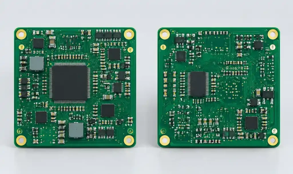
Boards assembled on both sides require fiducial strategy that works regardless of which side faces the camera. Place global fiducials symmetrically so they are visible from top and bottom—avoiding component shadow zones where placed components obstruct fiducial vision when the board flips for second-side assembly.
The recommended pattern: position fiducials in diagonal corners where tall components (connectors, inductors, electrolytic capacitors) are unlikely to populate. When component height exceeds 15mm on one side, verify fiducial visibility from the opposite side using 3D CAD analysis before releasing to production.
Some assembly houses require separate fiducial sets for each side—three fiducials visible only from top, three different fiducials visible only from bottom. This doubles fiducial count but eliminates visibility concerns and supports simultaneous top-bottom imaging in advanced inspection systems.
Rigid-Flex and Flex Circuit Fiducials
Flex circuits and rigid-flex boards experience 3-5× more dimensional variation than standard rigid PCBs due to material anisotropy and handling-induced distortion. Standard three-fiducial placement proves insufficient for flex sections exceeding 50mm length.
Add fiducials every 40-50mm along flex sections to create localized coordinate systems that accommodate non-uniform distortion. The vision system treats each segment independently, applying separate transformation matrices that account for differential stretch and twist.
Place rigid-flex fiducials on rigid sections only—never on flex regions where material flexibility prevents stable reference. When flex sections require local component fiducials, ensure the flex area is mechanically stabilized (tacked down, held in fixture) during vision acquisition and component placement.
Design Checklist for Production-Ready Fiducials
Fiducial Design Verification:
- 1mm diameter copper pad with 2mm solder mask clearance (or 0.5mm/1mm for compact designs)
- Bare copper surface—no ENIG, HASL, or OSP coverage in fiducial center
- 3mm minimum keep-out zone—no silkscreen, traces, or copper features
- Fiducials on same side as components they reference
- Fiducial copper isolated from ground planes by 5mm relief
Placement Verification:
- Three global fiducials forming non-collinear triangle
- Maximum diagonal separation (≥100mm for boards >150mm)
- 5mm minimum clearance from board edges and V-scores
- Local fiducials within 5mm of fine-pitch components (≤0.5mm pitch)
- Asymmetric pattern prevents 180° orientation errors
Panel and Multi-Board Considerations:
- Board-level fiducials in addition to panel rails for fine-pitch assembly
- Panel fiducials outside board outlines and V-score lines
- Fiducials remain with board after depaneling
- Double-sided assembly fiducials avoid component shadow zones
FAQ
How many fiducials do I need on a PCB?
Minimum three global fiducials for every board undergoing automated assembly. Add two local fiducials per component for BGAs with ≤0.5mm pitch, QFN packages, or 0201/01005 components. Boards exceeding 200mm in any dimension benefit from four to five global fiducials to compensate for increased thermal expansion and laminate warpage. Panels require three panel-level fiducials plus three board-level fiducials per individual board.
Can I use component pads as fiducials?
No. Component pads have solder mask coverage, irregular shapes, and positional tolerances that make them unsuitable optical references. IPC-7351B requires dedicated fiducial features with controlled geometry and maximum optical contrast. Using component pads as fiducials reduces placement accuracy by 40-60% and increases assembly defect rates. The 0.35mm² copper area consumed by a proper 1mm fiducial is insignificant compared to assembly yield improvement.
What happens if fiducials are missing or incorrect?
Missing fiducials force assemblers to manually create alignment references using component pads or board corners, reducing accuracy to ±0.15-0.25mm versus ±0.025-0.05mm with proper fiducials. This increases placement defects, solder bridging, and tombstoning, particularly for fine-pitch components. Incorrect fiducials (wrong size, insufficient clearance, collinear placement) cause vision system failures, production delays, and potential wrong-side component placement if orientation errors go undetected.
Do I need fiducials for hand assembly?
No. Fiducials are optical references for machine vision systems. Manual assembly uses mechanical tooling pins, alignment fixtures, or visual inspection of component pads. However, adding fiducials to hand-assembled prototypes facilitates later transition to automated assembly without board redesign. The minimal cost of adding fiducials to prototypes (no added fabrication cost) far outweighs redesign expenses when scaling to production.
Should fiducials have surface finish?
No surface finish on the fiducial copper pad center region—bare copper provides optimal optical contrast. Apply standard surface finish (ENIG, HASL, OSP) to component pads but exclude fiducial pads from surface finishing per IPC-7351B. Most fabricators handle this automatically when fiducials are designated correctly in Gerber files. The 2mm solder mask opening surrounding the 1mm copper pad receives standard solder mask, creating the high-contrast ring required for edge detection.
Conclusion
Proper fiducial mark placement is mandatory for reliable automated PCB assembly. Three non-collinear global fiducials at maximum diagonal spacing, combined with local fiducials for fine-pitch components, enable ±0.025mm placement accuracy required for modern high-density electronics. Following IPC-7351B dimensional standards (1mm copper, 2mm solder mask clearance) and maintaining 3mm clearance zones ensures vision system compatibility across all assembly equipment.
If you need high-quality PCB assembly for complex boards with fine-pitch BGAs, 01005 components, or HDI technology, Andwin Circuits offers advanced SMT capabilities with optical vision systems supporting up to 50-layer boards. Our facility follows IPC-A-610 Class 3 standards and provides fast turnaround in 7 days for prototype assemblies. We deliver first-article inspection, X-ray BGA verification, and comprehensive DFM review including fiducial placement optimization.
Contact us today for PCB assembly services, fiducial design verification, and technical consultation for your next electronics project.