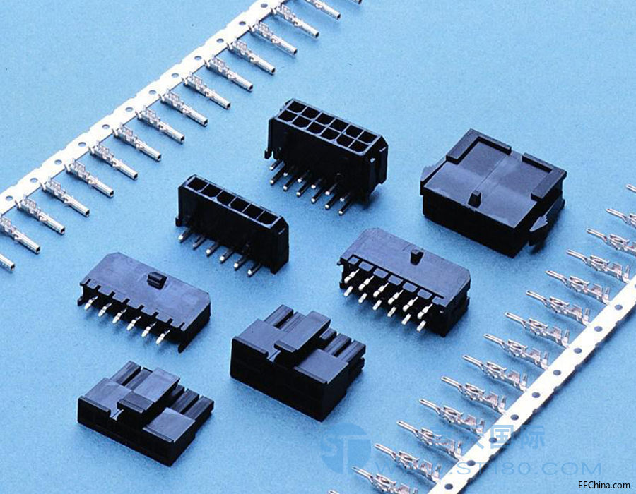
Through hole pcb assembly-DIP lines
Through hole PCB assembly is a process of assembling electronic components onto a printed circuit board (PCB) that involves inserting the leads of the components through holes in the board and then soldering them onto the opposite side of the board.
This method is commonly used for components that require a stronger mechanical connection or higher current carrying capacity than surface mount components.

The through hole assembly process typically involves the following steps:
1. Component insertion:
The components are inserted into the holes on the PCB using automated or manual insertion equipment.
2. Wave soldering:
The PCB is passed through a wave soldering machine where a wave of molten solder is used to solder the component leads to the opposite side of the board.
3. Inspection:
The assembled PCB is inspected for any defects or issues before moving on to the next stage.

4. Testing:
The PCB is tested to ensure that it functions correctly and meets the required specifications.
Through hole PCB assembly is a reliable and widely used method for assembling electronic components onto a PCB.
However, it is generally slower and more expensive than surface mount assembly due to the additional steps involved in the process.

Control the quality of through hole pcb assembly:
Through hole PCB assembly quality control involves a series of steps and measures to ensure that the final product meets the required standards and specifications. Some of the key quality control measures include:
1. Visual Inspection:
The first step in quality control is a visual inspection of the PCB assembly. This involves checking for any visible defects such as solder bridges, cold solder joints, and missing components.
2. Soldering Quality:
The quality of the soldering is critical to the performance of the PCB. The solder joints should be smooth and shiny, with no signs of cracking or voids.
3. Component Placement:
The placement of components on the PCB should be accurate and consistent. This ensures that the components are properly aligned and that there is no risk of short circuits or other issues.

4. Electrical Testing:
Once the PCB is assembled, it should be subjected to electrical testing to ensure that it functions as intended. This involves testing for continuity, resistance, and other electrical properties.
5. Environmental Testing:
PCBs are often subjected to harsh environments, so it is important to test them under different conditions to ensure that they can withstand temperature changes, humidity, and other factors.
6. Documentation:
Finally, all quality control measures should be documented to ensure that the PCB assembly meets the required standards and specifications. This includes documenting the inspection and testing results, as well as any corrective actions taken.


