A brief analysis of the reliability of printed circuit boards
One of the basic functions of printed circuit boards is to carry the transmission of electrical signals.
The study of the reliability of printed circuit boards is to study whether its basic functions are not lost or some of its electrical performance indicators are not decayed, that is, the durability of its functions. This paper intends to study the reliability of printed circuit boards from three aspects: the quality of printed circuit boards after installation by downstream users, the quality of direct user debugging, and the quality of product use, so as to characterize the quality of printed circuit board processing and provide a basic way to produce high-reliability printed circuit boards.
1 Reliability analysis of printed circuit boards
1.1 Quality characterization after installation of printed circuit boards
After the installation of printed circuit boards, the quality of the printed circuit boards is directly reflected by:
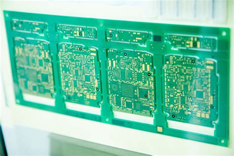
Visually inspect whether the printed circuit boards have bubbling, white spots, warping, etc.
The most concerning one is bubbling, which is called “explosion or delamination” by industry insiders. High-reliability printed circuit boards should not have “bubbling” defects after installation. In order to obtain high-reliability printed circuit boards, it is necessary to start from the following aspects.
1.1.1 Selection of printed circuit board materials
The same type of printed circuit board substrate has different performance differences from different manufacturers, and the performance differences of different types of printed circuit board substrates are even greater. When selecting substrates for printed circuit board processing, both the heat resistance and electrical properties of the materials should be considered. As for installation, we consider the heat resistance of the materials more. The heat resistance of the material is generally based on the glass transition temperature (Tg) and thermal decomposition temperature (Td). At present, printed circuit board installation is divided into lead, lead-free, and mixed installation according to the solder joint composition of components (lead, lead-free), and the corresponding reflow peak temperature is 215 ℃, 250 ℃, and 225 ℃. Therefore, for different installation methods, printed circuit board materials should be selected separately. For lead-free soldering, select boards with a Tg higher than 170 ℃; for mixed soldering, select boards with a Tg higher than 150 ℃.
For lead soldering, all materials are applicable, but boards with a Tg higher than 130 ℃ are usually selected. In addition to considering Tg, we should also pay attention to the manufacturer’s brand and model. At present, the commonly used boards with relatively stable performance include Tuc, IsoIa, Hitachi, Neleo, etc.
1.1.2 Control of the production process
Before leaving the factory, the printed circuit board must be sampled for acceptance and thermal stress tests, the purpose of which is to ensure that the installation is not layered. Although products that are completely qualified in the acceptance and thermal stress tests cannot guarantee that there are no defects in the installation, there are definitely hidden dangers when installing products with defects in the acceptance state. Therefore, the acceptance and thermal stress tests are the early warning of the installation quality. In this way, the acceptance and thermal stress are the necessary conditions for the delivery of the printed circuit board. For this reason, the following aspects should be paid attention to during the processing of the printed circuit board to ensure that the acceptance and thermal stress tests are qualified and improve the quality after installation.
1.1.2.1 Clarify the processing requirements of the printed circuit board
The number of layers, thickness, BGA pitch (or the minimum center distance between the hole walls), conductor copper thickness, etc. of the printed circuit board affect the results of the thermal stress test of the printed circuit board. For boards with more than 12 layers and a thickness greater than 3.0 mm, microcracks and hole wall defects are easily generated after thermal stress due to the large Z-axis expansion and contraction value.
When the BGA pitch is less than 0.8 mm or the hole wall center distance is less than 0.5 mm, due to the large heat capacity, the heat is concentrated during installation, which is easy to cause dielectric layer delamination. Therefore, for this type of printed circuit board processing, a substrate with a Tg greater than 170 ℃ should be selected.
When the conductor thickness is greater than 35 μm, the heat capacity is large, and the resin flow resistance is large, multiple high-flow prepregs should be used as much as possible during lamination. For printed circuit boards with a hole diameter less than 0.3 mm, the quality of drilling directly affects the quality of the hole wall. The drilling parameters should be strictly controlled to ensure that the hole wall is clean, flat, and tear-free.
1.1.2.2 Refined process control
When delamination occurs in the delivery state and thermal stress test, the main reason is that the quality defects of the inner conductor oxidation treatment cause poor bonding between copper and prepreg or the prepreg is contaminated or absorbs moisture. The oxidation process varies depending on the material. High Tg materials are hard and brittle, so velvety brown oxidation is used, while conventional materials may be crystalline black oxidation [2]. Of course, the roughness of the conductor surface directly affects the bonding strength between copper and prepreg. Therefore, no matter what kind of oxidation treatment is used, the surface roughness of the oxidation must be clearly specified. At the same time, during the lamination process, the contamination and moisture absorption of the material should be avoided as much as possible. To this end, the baking conditions of the single sheet must be quantitatively controlled, the prepreg must be dehumidified, and the cleanliness and operation specifications of the environment must be controlled during the stacking. In the lamination process control, effective lamination parameters must be established according to the board type and board quantity to ensure that the resin is fully wetted and the rheological speed is maintained to avoid the generation of voids.
1.2 Characterization of the quality of printed circuit board debugging
The quality of printed circuit board debugging is mainly based on whether the debugging results meet the design requirements smoothly. Whether the printed circuit board is debugged smoothly after installation involves the processing quality of the printed circuit board and is also an important information for characterizing the reliability of the printed circuit board. Generally speaking, a board that is debugged smoothly has high reliability; on the contrary, a board that is not debugged smoothly must have hidden dangers in its reliability. The processing quality of the printed circuit board mainly involves the wires, disks, and dielectric layers of the printed circuit board.
1.2.1 The influence of printed circuit board conductors on the quality of printed circuit boards
With the development of sophisticated electronic products and the continuous improvement of printed circuit board processing technology, the conductors of printed circuit boards are no longer simple signal transmission, but are supplemented by many functional requirements such as impedance lines, equal length lines, and reactance lines. Therefore, the defects of the conductors such as notches, burrs, and shape corners have an increasingly obvious impact on the performance of the printed circuit board (3). A 10% deviation in line width may bring about an impedance change of up to 20%. The notches and burrs of the conductors may cause the signal delay to reach 0.1 ns. The difference in the shape of the conductors produces interference such as reflection and noise, which affects the integrity of signal transmission. It can be seen that the quality of the wire cannot be ignored in the process of printed circuit board production. On the one hand, this requires strict process control, and on the other hand, it requires high-precision production equipment and appropriate process technology (such as semi-additive method and additive method) to ensure that the accuracy of the wire meets the design requirements.