A Brief Discussion on PCB Teardrops
Abstract
In printed circuit board (PCB) design, teardrops (or teardropping) are a crucial technique used to enhance the reliability and manufacturability of PCB traces, particularly at the junctions between traces and pads or vias. This paper explores the concept of PCB teardrops, their benefits, implementation methods, and considerations in modern PCB design. The discussion covers their role in preventing manufacturing defects, improving mechanical strength, and optimizing signal integrity.
1. Introduction
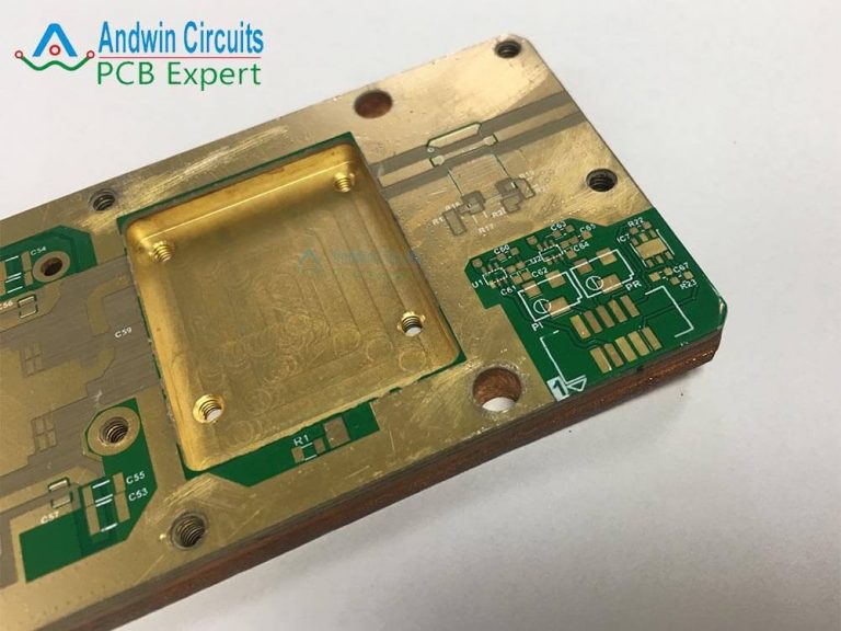
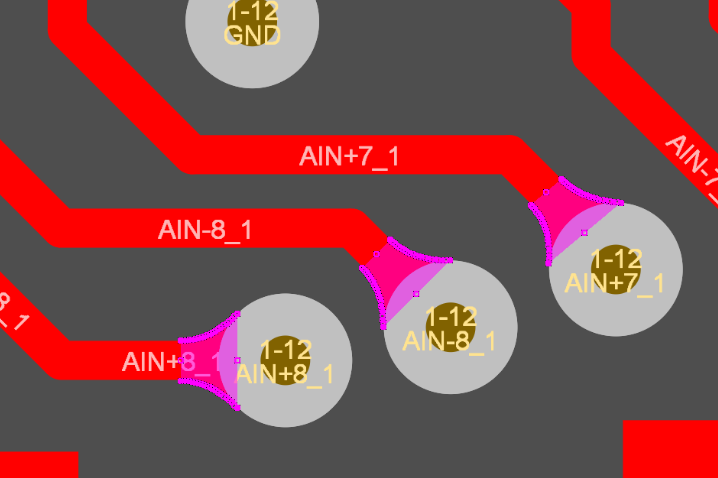
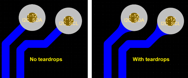
A printed circuit board (PCB) is the backbone of most electronic devices, providing mechanical support and electrical connections between components. One of the subtle yet significant design techniques in PCB layout is the use of teardrops. A teardrop is a tapered transition between a thin trace and a wider pad or via, resembling the shape of a teardrop.
While seemingly minor, teardrops play a critical role in ensuring PCB reliability, especially in high-density and high-frequency designs. This paper examines why teardrops are used, their advantages, and how they are implemented in modern PCB design software.
2. The Purpose of Teardrops in PCB Design
2.1 Preventing Manufacturing Defects
During PCB fabrication, especially in processes like drilling and etching, misalignment can occur between traces and pads/vias. If a thin trace connects abruptly to a pad, the drill bit may partially remove the copper, leading to weak connections or open circuits. Teardrops mitigate this risk by providing a smooth, reinforced transition.
2.2 Enhancing Mechanical Strength
PCBs undergo mechanical stress during assembly, soldering, and operation. A sharp junction between a trace and a pad is more prone to cracking under stress. Teardrops distribute mechanical forces more evenly, reducing the likelihood of trace fractures.
2.3 Improving Signal Integrity (High-Speed Design)
In high-frequency PCB designs, impedance discontinuities can cause signal reflections. While teardrops primarily serve a mechanical purpose, they can also help maintain consistent trace widths near vias, minimizing impedance variations.
2.4 Aiding in Acid Trapping Prevention
During PCB etching, chemicals can sometimes “trap” in sharp corners, leading to over-etching. Teardrops reduce such risks by smoothing out transitions.
3. Types of Teardrops
There are two primary types of teardrops in PCB design:
- Pad-to-Trace Teardrops – Applied where a trace connects to a component pad.
- Via-to-Trace Teardrops – Applied where a trace connects to a via.
Some advanced designs also use curved teardrops for high-frequency applications to further minimize impedance discontinuities.
4. Implementation of Teardrops
Most modern PCB design software (e.g., Altium Designer, KiCad, Cadence Allegro) includes automated teardrop generation tools. The key parameters for teardrop implementation include:
- Length – The extension of the teardrop along the trace.
- Width – The maximum width of the teardrop at the pad/via junction.
- Shape – Linear or curved transitions.
4.1 Manual vs. Automatic Teardropping
- Manual Teardropping: Used in older or highly customized designs, where the designer manually adds copper pours.
- Automatic Teardropping: Modern EDA tools allow batch application of teardrops, saving time and ensuring consistency.
5. When to Use (and Avoid) Teardrops
5.1 Recommended Cases
- High-density interconnect (HDI) PCBs
- Flexible PCBs (where mechanical stress is higher)
- High-reliability designs (e.g., aerospace, medical devices)
- Designs with fine-pitch components
5.2 Cases Where Teardrops May Be Unnecessary
- Very large traces that already have sufficient strength
- Low-frequency or low-cost consumer PCBs where reliability is less critical
- When space constraints prevent their use
6. Potential Challenges and Considerations
While teardrops offer many benefits, improper use can lead to issues:
- Increased Capacitance: In extremely high-speed designs, teardrops might introduce slight parasitic capacitance.
- Space Constraints: In ultra-high-density designs, teardrops may consume valuable routing space.
- Aesthetic Concerns: Some designers prefer cleaner-looking traces without teardrops for simplicity.
7. Conclusion
Teardrops are a small but powerful feature in PCB design that significantly enhance manufacturability, mechanical robustness, and signal integrity. While not always mandatory, their strategic use can prevent costly failures in high-reliability applications. As PCB technology advances, automated teardrop tools in EDA software make their implementation easier than ever.
Designers should evaluate whether teardrops are necessary based on their specific application, balancing reliability needs with design constraints. By understanding and applying teardrops effectively, PCB engineers can improve both the quality and longevity of their electronic products.