A brief discussion on the causes and processes of PCB size expansion and contraction
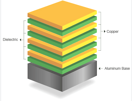
During the process of transferring the inner layer circuit pattern from the substrate once, through several laminations, to the outer layer circuit pattern transfer, different expansion and contraction in the warp and weft directions of the panel will occur.
From the entire PCB production FLOW-CHART, we can find out the reasons and processes that may cause abnormal expansion and contraction of panels and poor dimensional consistency:
1.Dimensional stability of incoming substrate materials, especially the dimensional consistency between each lamination CYCLE of the supplier; even if the dimensional stability of different CYCLEs of the same specification substrate is within the specification requirements, due to the poor consistency between them, it may cause the pattern size of subsequent batch production panels to exceed the tolerance after the first trial production of the panel determines a reasonable inner layer compensation; at the same time, there is another material abnormality that is the shrinkage of the panel during the process from the transfer of the outer layer pattern to the shape process; in the production process, some batches of panels were found to have serious shrinkage in the width of the panel and the length of the shipping unit relative to the transfer ratio of the outer layer pattern during the data measurement before the shape processing, with a ratio of 3.6mil/10inch. The specific data is shown in the table below; after investigation, the X-RAY measurement of the abnormal batch of panels after the outer layer lamination and the outer layer pattern transfer ratio are both within the control range, and are currently under process monitoring. There is still no better way to monitor;
2.Panel design: The panel design of conventional panels is symmetrical, and there is no obvious effect on the graphic size of the finished PCB when the graphic transfer ratio is normal; however, some panels use asymmetrical structure design in the process of improving sheet material utilization and reducing costs, which will have a very obvious impact on the consistency of graphic size of finished PCBs in different distribution areas. Even in the process of PCB processing, we can find that the alignment of such asymmetrically designed panels in each link is more difficult to control and improve than conventional panels during laser blind hole drilling and outer layer graphic transfer exposure/solder mask exposure/character printing;
3.One-time inner layer graphic transfer process: This plays a very critical role in whether the size of the finished PCB board meets customer requirements; if there is a large deviation in the film ratio compensation of the one-time inner layer graphic transfer, it can not only directly lead to the finished PCB graphic size failing to meet customer requirements, but also cause the subsequent laser blind hole and its bottom connection plate to align abnormally, resulting in LAYER TO The insulation performance between LAYERs deteriorates until short circuit, and the through/blind hole alignment problem during the transfer of the outer layer graphics;
Based on the above analysis, we can take appropriate measures to monitor and improve the abnormalities;
1.Monitoring the dimensional stability of incoming substrates and the dimensional consistency between batches: Regularly conduct dimensional stability tests on substrates provided by different suppliers, and track the differences in the warp and weft data between different batches of the same specification sheets, and appropriately use statistical techniques to analyze the substrate test data; thereby, it is also possible to find suppliers with relatively stable quality, and provide more detailed supplier selection data for SQE and procurement departments; for individual batches of poor substrate dimensional stability causing panels in The serious expansion and contraction after the transfer of the outer layer graphics can only be discovered by measuring the first board of the appearance production or during the shipment review; but the latter has high requirements for batch management, and it is easy to mix boards when a certain number is produced in large quantities;
2.The design of the panel should adopt a symmetrical structure design scheme to keep the expansion and contraction of each shipping unit in the panel relatively consistent; if possible, communicate with the customer and suggest that they allow the position of each shipping unit in the panel to be specifically marked by etching/characters on the process edge of the panel; this method will be more effective in asymmetrically designed panels, even if the individual units in each panel have size deviations due to asymmetric graphics, or even the bottom connection of local blind holes caused by this It is also very convenient to identify abnormal units and pick them out before shipment, so that they will not flow out and cause abnormal packaging of customers and cause complaints;
3.Make the first board with magnification, and scientifically determine the first inner layer pattern transfer magnification of the production board through the first board; this is particularly important when changing other suppliers’ substrates or P sheets to reduce production costs; when it is found that a board is out of control, it should be determined whether its unit tube hole is a secondary drilling process; if it is a conventional processing flow board, it can be released according to the actual situation to the outer layer pattern transfer through the film magnification for appropriate adjustment; if it is a secondary drilling board, the handling of abnormal boards must be particularly cautious to ensure that the pattern size of the finished board is consistent with the target to the tube hole (secondary drilling) Distance; attached is a list of the first board ratios of secondary laminated boards;
4.Process monitoring: Use the inner layer target data of the board measured by the X-RAY production of the outer or second outer board after lamination to analyze whether it is within the control range and compare it with the corresponding data collected by the qualified first board to determine whether the board size has abnormal expansion and contraction. The attached table is for reference; after theoretical calculation, the ratio here should usually be controlled within +/-0.025% to meet the size requirements of conventional boards;
By analyzing the reasons for the expansion and contraction of PCB size, we can find out the available monitoring and improvement methods. We hope that the majority of PCB practitioners can get inspiration from it and find improvement solutions suitable for their own companies based on their actual conditions.