A comprehensive analysis of main printed circuit board (pcb)assembly
Introduction
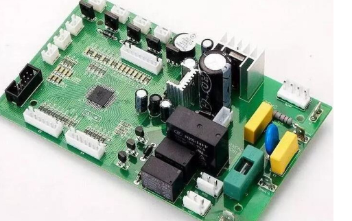
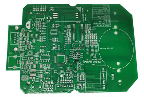
In modern electronic devices, the printed circuit board (PCB) is one of the core components, responsible for connecting and supporting various electronic components to ensure the normal operation of the device. As the core part of the electronic device, the main printed circuit board (Main PCB) carries key electronic components and circuits, and its assembly quality directly affects the performance and reliability of the device. This article will explore the various aspects of the main PCB assembly in depth, including design, material selection, assembly process, testing and quality control, etc., aiming to provide readers with a comprehensive understanding.
1.Design of the main PCB
1.1 Circuit design
The design of the main PCB begins with circuit design. According to the functional requirements of the device, the circuit designer draws the circuit diagram and determines the connection method and signal path of each electronic component. Circuit design needs to consider factors such as signal integrity, power supply stability, and electromagnetic compatibility (EMC).
1.2 PCB layout
After the circuit design is completed, the next step is PCB layout. The layout designer places the components in the circuit diagram on the PCB board and plans the routing path of the signal line and power line. The layout design needs to consider the following factors:
Component placement: high-frequency components should be placed as close as possible to reduce signal transmission delay; heat-generating components should be placed in a dispersed manner to avoid local overheating.
Signal integrity: high-speed signal lines should be as short and straight as possible, avoiding crossing and loops to reduce signal reflection and crosstalk.
Power and ground lines: power and ground lines should be as wide as possible to reduce resistance and inductance and ensure power supply stability.
1.3 PCB wiring
Wiring is the last step in PCB design. Designers actually draw signal lines and power lines on the PCB board according to the layout plan. The wiring needs to consider the following factors:
Signal layer and power layer: multi-layer PCBs usually have dedicated signal layers and power layers to optimize signal transmission and power distribution.
Impedance control: high-speed signal lines need to be impedance controlled to ensure the integrity of signal transmission.
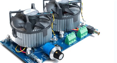
Heat dissipation design: for high-power components, heat dissipation holes or heat sinks need to be designed on the PCB to improve heat dissipation efficiency.

2.Material selection
2.1 PCB substrate material
The selection of PCB substrate material has an important impact on the performance of the PCB. Common substrate materials include:
FR-4: A common glass fiber reinforced epoxy resin material with good mechanical strength and electrical properties, suitable for most applications.
High-frequency materials: such as polytetrafluoroethylene (PTFE), suitable for high-frequency circuits, with low dielectric constant and low loss tangent.
Metal substrates: such as aluminum substrates, with good heat dissipation performance, suitable for high-power applications.
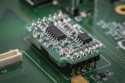
2.2 Electronic components
The selection of electronic components directly affects the performance and reliability of PCBs. Common electronic components include:
Resistors, capacitors, inductors: used to regulate current, voltage and signals in circuits.
Integrated circuits (ICs): such as microprocessors, memories, amplifiers, etc., are the core components of PCBs.
Connectors: used to connect PCBs to other devices or modules.
2.3 Welding materials
Welding materials are used to fix electronic components on PCBs. Common welding materials include:
Solder: usually tin-lead alloy or lead-free solder, used to form electrical connections and mechanical fixation.
Solder paste: used in surface mount technology (SMT), components are soldered on PCB by reflow soldering.
3.Assembly process
3.1 Surface mount technology (SMT)
SMT is the main process of modern PCB assembly, suitable for miniaturized and high-density integrated electronic components. The main steps of SMT include:
Solder paste printing: solder paste is printed on the pads of PCB through steel mesh.
Component placement: electronic components are accurately placed on solder paste using a placement machine.
Reflow soldering: the PCB is passed through a reflow soldering oven, the solder paste melts and forms a reliable solder connection.
3.2 Through-hole technology (THT)
THT is suitable for electronic components that are larger or require high mechanical strength. The main steps of THT include:
Component insertion: the pins of the component are inserted into the through holes of the PCB.
Wave soldering: the PCB is passed through a wave soldering machine, the solder melts and forms a solder connection.
3.3 Manual soldering
For some special components or small batch production, manual soldering can be used. Manual soldering requires skilled techniques to ensure soldering quality and reliability.
4.Testing and quality control
4.1 Automated Optical Inspection (AOI)
AOI automatically detects soldering defects on PCBs, such as cold soldering, short circuits, and misalignment, through high-resolution cameras and image processing software. AOI can greatly improve detection efficiency and accuracy.
4.2 In-circuit Testing (ICT)
ICT automatically detects circuit open circuits, short circuits, component values, and other parameters by contacting the test points on the PCB with test probes. ICT can quickly locate fault points and improve production efficiency.
4.3 Functional Testing
Functional testing is a comprehensive functional verification of the assembled PCB to ensure that it meets the design requirements. Functional testing usually includes power testing, signal testing, communication testing, etc.
4.4 Environmental Testing
Environmental testing is used to evaluate the reliability of PCBs under different environmental conditions, including temperature cycle testing, humidity testing, vibration testing, etc. Environmental testing can detect potential design defects in advance and improve product reliability.
5.Future Development Trends
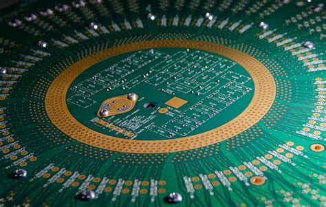
5.1 High Density Interconnect (HDI)
With the miniaturization and high performance of electronic devices, HDI technology has attracted more and more attention. HDI PCB achieves higher wiring density and smaller size through microvia, blind via and buried via technology.
5.2 Flexible PCB
Flexible PCB uses flexible substrate materials, which can be bent and folded, and is suitable for special applications such as wearable devices and medical devices. The design and assembly process of flexible PCB is different from that of traditional rigid PCB, requiring special technology and equipment.
5.3 Green Manufacturing
With the improvement of environmental awareness, green manufacturing has become an important trend in the PCB industry. Green manufacturing includes the use of lead-free solder, environmentally friendly substrate materials, energy-saving production processes, etc. to reduce the impact on the environment.
Conclusion
The main PCB assembly is a complex and sophisticated process involving multiple links such as design, material selection, assembly process, testing and quality control. Each link requires strict control and delicate operation to ensure the performance and reliability of the PCB. With the continuous advancement of technology, the PCB assembly process is also constantly developing and innovating, and will develop in the direction of high density, flexibility and green manufacturing in the future. By deeply understanding and mastering each link of main PCB assembly, we can better cope with future challenges and promote the continuous advancement of electronic devices.