A Comprehensive Guide to Creating Castellated Holes (Stamp Holes) in PCB Design
Introduction
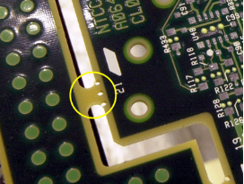
Printed Circuit Board (PCB) design involves various techniques to ensure proper connectivity, mechanical stability, and manufacturability. One such technique is the use of castellated holes, also known as stamp holes, which allow PCBs to be mounted onto another board like a surface-mount component. These half-plated holes along the edges of a PCB enable easy soldering and modular assembly.
This article provides a step-by-step guide on how to design and implement castellated holes in PCB layouts, covering their purpose, design considerations, manufacturing process, and best practices.
1. What Are Castellated Holes (Stamp Holes)?
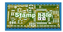
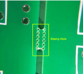
Castellated holes are plated half-holes drilled along the edges of a PCB, resembling the perforations on a postage stamp (hence the name “stamp holes”). They are commonly used in:
- Module PCBs (Wi-Fi, Bluetooth, RF modules)
- Breakaway board designs (for panelization)
- Board-to-board soldering (allowing one PCB to be soldered onto another like an SMD component)
These holes provide both electrical connections and mechanical support, eliminating the need for connectors in some cases.
2. Design Considerations for Castellated Hole
2.1. Hole Size and Spacing
- Diameter: Typically ranges from 0.6 mm to 1.0 mm, but depends on the application.
- Spacing (Pitch): Usually 1.27 mm (0.05″) or 2.54 mm (0.1″), matching standard header spacing.
- Plating Thickness: Should be sufficient for soldering (typically 20-30 µm copper plating).
2.2. PCB Edge Clearance
- Ensure the holes are placed close enough to the edge so that when the PCB is cut, half of the hole remains.
- A 0.2–0.3 mm margin from the board edge is typical.
2.3. Soldering Pads
- Add solder mask openings around the holes to ensure proper solder wetting.
- Optional: Include thermal relief pads to prevent heat dissipation during soldering.
2.4. Panelization and Breakaway Tabs
- If the PCB is part of a larger panel, include mouse bites (breakaway tabs) for easy separation.
- Ensure the castellated holes are aligned correctly after depaneling.
3. Step-by-Step Guide to Designing Castellated Holes
3.1. PCB Design Software Setup
Most PCB design tools (Altium Designer, KiCad, Eagle, OrCAD) support castellated hole design. The general steps include:
- Define the Board Outline:
- Draw the PCB outline where the castellated holes will be placed.
- Place Drilled Holes Near the Edge:
- Add plated through-holes (PTH) along the intended edge.
- Ensure the holes are partially outside the board outline (so they become half-holes after routing).
- Adjust Board Edge to Cut the Holes in Half:
- Use a milling or routing path that cuts through the center of the holes.
3.2. Gerber File Preparation
- Drill File (Excellon): Contains hole drilling data.
- Board Outline (GKO/GTL/GTS): Defines the final shape after cutting.
- Copper and Solder Mask Layers: Ensure proper pad exposure.
3.3. Manufacturer Specifications
- Clearly indicate castellated holes in fabrication notes.
- Specify “half-cut plated holes” or “castellated edges” in the order.
4. Manufacturing Process for Castellated Holes
4.1. Drilling and Plating
- Drill Full Holes: Standard PTH drilling is performed.
- Copper Plating: Holes are electroplated to ensure conductivity.
4.2. Routing the PCB Edge
- A CNC router cuts the board edge, splitting the holes in half.
- The remaining half-holes retain their plating, allowing soldering.
4.3. Quality Control
- Inspect for proper plating adhesion.
- Ensure no copper peeling at the cut edges.
5. Soldering Castellated Modules
- Solder Paste Application: Apply paste to the pads on the main PCB.
- Placement: Align the castellated module and reflow solder.
- Inspection: Check for bridging or cold joints.
6. Advantages and Disadvantage
6.1. Advantages
✔ Space-Saving: Eliminates the need for connectors.
✔ Cost-Effective: Reduces component count.
✔ Modular Design: Allows easy replacement of modules.
6.2. Disadvantages
✖ Limited Reusability: Difficult to desolder without damage.
✖ Manufacturing Complexity: Requires precise milling.
7. Best Practices
✅ Use Standard Hole Sizes for compatibility.
✅ Include Fiducial Marks for alignment.
✅ Test Prototypes before mass production.
Conclusion
Castellated holes (stamp holes) are a valuable PCB design feature for modular electronics, enabling easy board-to-board soldering. Proper design, manufacturing, and soldering techniques ensure reliable connections. By following this guide, engineers can effectively implement castellated holes in their PCB projects.
Would you like additional details on specific CAD tools or manufacturing techniques? Let me know how I can further assist your PCB design process!