A PCB anti-interference design technology for high-speed DSP
In recent years, with the rapid development of new processes and new devices, high-speed devices have become more and more popular, and high-speed circuit design has become a commonly needed technology. TI’s DSPs chip TMS320C62xx, C64xx, and C67xx series devices are one of the rapidly developing high-speed devices. The internal structure of C6000 is fixed-point, and the floating-point series is compatible with DSP. The current CPU main frequency is 100MHz, -4i00MHz.
It has VelociTITM’s advanced very long instruction word (VLIW) structure core, which can execute 8 32-bit instructions in parallel in one instruction cycle. Due to its high-speed computing capability, it is widely used in communications, electronic countermeasures, radars, image processing, and other fields that require highly intelligent and high-speed processing capabilities.
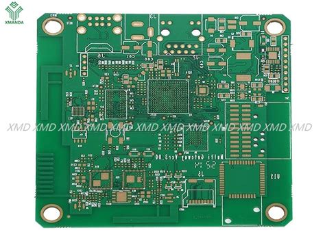
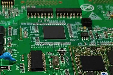
As the chip integration becomes higher and higher, the number of chip pins is also increasing, and the packaging of devices is also constantly changing, from DIP to OSOP, from SOP to PQFP, and from PQFP to BGA. TMS320C6000 series devices use BGA packaging. In terms of circuit application, BGA packaging has the characteristics of high success rate, low repair rate and high reliability, and its application is becoming more and more extensive. However, since BGA packaging belongs to ball grid array patch packaging, the physical implementation of the system under development, that is, board-level design, involves many high-speed digital circuit design technologies. In high-speed systems, the generation of noise interference is the first influencing factor. High-frequency circuits will also generate radiation and conflict, while faster edge rates will generate ringing, reflection and crosstalk. If the particularity of high-speed signal layout and routing is not considered, the designed circuit board will not work properly. Therefore, the successful design of PCB boards is a very critical link in the DSPs circuit design process.
1 Transmission line effect
1.1 Signal integrity
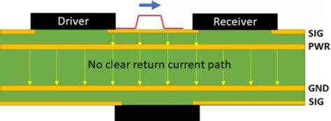
Signal integrity mainly includes reflection, ringing, ground bounce and crosstalk. The traces on the PCB board can be equivalent to the series and parallel capacitor, resistor and inductor structure shown in Figure 1. The typical value of the series resistor is 0.25D./R-4). 55DJft, and the parallel resistor value is usually very high. After adding parasitic resistance, capacitance and inductance to the actual PCB connection, the final impedance on the connection is called characteristic impedance zo. If the impedance of the transmission line and the receiving end do not match, this will cause reflection and oscillation of the signal.
Changes in wiring geometry, incorrect line termination, transmission through connectors and discontinuity of power planes can all lead to reflections. Overshoot and undershoot are generated when the signal changes at the rising and falling edges of the level, which will instantly produce glitches above or below the steady level, which can easily damage the device. The ringing and surround oscillation of the signal are caused by improper inductance and capacitance on the line respectively. Ringing can be reduced by proper termination. When there is a large current surge in the circuit, it will cause ground bounce. If there is a large transient current flowing through the power plane between the chip and the board, the parasitic inductance and resistance between the chip package and the power plane will cause power noise.
Crosstalk is a coupling problem between two signal lines. The mutual inductance and mutual capacitance between the signal lines cause noise on the line. Capacitive coupling causes coupling current, while inductive coupling causes coupling voltage. PCB board layer parameters, signal line spacing, electrical characteristics of the driver and receiver, and line termination methods all have a certain impact on crosstalk.
1.2 Solutions
Some measures to solve common problems:
The power layer does not restrict the direction of the current, and the return line can follow the path with the minimum impedance, which is the closest to the signal line. This may minimize the current loop, which will be the preferred method for high-speed systems. However, the power layer does not exclude line noise, and if the power distribution path is not paid attention to, all systems will generate noise and cause errors.
Therefore, special filters are required, which are implemented by bypass capacitors. Generally, a capacitor of 1p.F to 10p.F is placed at the power input end of the board, and a capacitor of 0.01p.F to U0.1 is placed between the power and ground pins of each active device on the board. The bypass capacitor acts like a filter. A large capacitor (10aF) is placed at the power input to filter out the low-frequency (60Hz) noise generated outside the board. The noise generated by the active devices on the board will generate harmonics at a frequency of 100MHz or higher.
The bypass capacitor placed between each chip is usually much smaller than the capacitor placed at the power input of the board. According to experience, if the design is mixed with analog and digital, the PCB is divided into analog and digital parts, analog devices are placed in the analog part, digital devices are placed in the digital part, and A/D converters are placed across the area. Analog signals and digital signals are wired in their respective areas to ensure that the return current of the digital signal does not flow into the ground of the analog signal. Bypass and decoupling are to prevent energy from being transferred from one loop to another. The three loop areas of the power layer, the bottom layer, the components and the internal power connection need to be paid attention to. Try to widen the width of the power supply and ground wires. It is best that the ground wire is wider than the power supply wire. The relationship between them is: ground wire>power supply wire>signal wire. Usually the signal wire width is: 0.2~0.3mm, and the thinnest width can reach 0.05″-‘0.07mm. The power line is 1.2″-‘2.5 n’Lrfl. Use a large area of copper layer as the ground wire, and connect all unused areas on the printed circuit board to the ground as the ground wire.
Or make a multi-layer board, with the power supply and ground wire each occupying one layer. Configure a 0.01 core ceramic capacitor for each integrated circuit chip. If the printed circuit board space is small and cannot be installed, a 1~10 core tantalum electrolytic capacitor can be configured for every 4~10 chips. The high-frequency impedance of this device is particularly small, and the impedance is less than 1Q in the range of 500kI-Iz~20MHz, and the leakage current is very small (below 0.5LlA). Decoupling filter capacitors must be installed close to the integrated circuit, striving for the shortest capacitor leads and the smallest transient current loop area, especially high-frequency bypass capacitors cannot have leads.
When the system operates at 50MHz, transmission line effects and signal integrity problems will occur. Traditional measures can achieve relatively satisfactory results; when the system clock reaches 120MHz, it is necessary to consider the use of high-speed circuit design knowledge, otherwise the PCB designed based on traditional methods will not work properly. Therefore, high-speed PCB circuit design has become a design technology that electronic system designers must master.
2 PCB high-speed signal circuit design technology
2.1 High-speed signal wiring
The use of multi-layer boards for high-speed signal wiring is both a necessity for wiring and an effective means to reduce interference. It is necessary to reasonably select the number of layers to reduce the size of the printed board, make full use of the middle layer to set up the shield, and achieve nearby grounding, which can effectively reduce parasitic inductance, shorten the signal transmission length, reduce cross interference between signals, etc. All of these are beneficial to the reliability of high-speed circuits. According to data, when the same material is used, the noise of a four-layer board is 20dB lower than that of a double-layer board. The fewer bends in the lead, the better. It is best to use a full straight line. If a turn is required, a 45-degree fold line or arc turn can be used to reduce the external transmission and mutual coupling of high-speed signals, and reduce signal radiation and reflection.
The shorter the lead between the pins of high-speed circuit devices, the better. The longer the lead, the greater the distributed inductance and distributed capacitance, which will cause reflection and oscillation in the high-speed circuit system. The fewer the alternations between the lead layers between the pins of high-speed circuit devices, the better, that is, the fewer vias used in the component connection process, the better. According to measurements, a via can bring about 0.5pF of distributed capacitance, resulting in a significant increase in the delay of the circuit.
When wiring high-speed circuits, pay attention to the “cross interference” introduced by the close parallel routing of signal lines. If parallel distribution cannot be avoided, a large area of ”ground” can be arranged on the reverse side of the parallel signal lines to reduce interference. In two adjacent layers, the routing direction must be perpendicular to each other.
Measures to surround particularly important signal lines or local units with ground wires. Protective ground wires can be added to the periphery of signal lines that are not easily disturbed, such as clock signals and high-speed analog signals, to sandwich the signal lines to be protected. All types of signal lines cannot form loops, and ground wires cannot form current loops. If a loop wiring circuit is generated, it will cause great interference in the system. Daisy chain wiring can effectively avoid the formation of loops during wiring. One or more high-frequency decoupling capacitors should be set near each integrated circuit block. When analog ground wires, digital ground wires, etc. are connected to the common ground wire, a high-frequency choke link should be used. Some high-speed signal lines should be specially handled: differential signals are required to be on the same layer and as close to parallel wiring as possible. No signal is allowed to be inserted between differential signal lines, and they are required to be of equal length.
High-speed signal wiring should try to avoid branching or forming stubs. High-frequency signal lines running on the surface are prone to generate large electromagnetic radiation. When high-frequency signal lines are routed between the power supply and the ground wire, the radiation generated will be greatly reduced through the absorption of electromagnetic waves by the power supply and the bottom layer.
2.2 High-speed clock signal wiring
Clock circuits play an important role in digital circuits. C64xDSP is the latest member of the C6000 platform, and it has a sufficiently high processing speed. The high-speed clock of C64xDSP can reach 1.1GHz, which is 10 times that of the early C62xDSP. Therefore, in the future DSP modern electronic system application design, the requirements for clock wiring will become higher and higher. The high-speed clock signal line has the highest priority. Generally, when wiring, the main clock signal line of the system needs to be given priority. The high-speed clock signal line has a high signal frequency, and the routing is required to be as short as possible to ensure the minimum distortion of the signal.
High-frequency clocks are particularly sensitive to noise interference. High-frequency clock signal lines need to be protected and shielded to minimize interference.
High-frequency clocks (clocks above 20MHz, or clocks with a rising edge of less than 5ns) must be escorted by ground wires. The line width of the clock is at least 10rail, and the line width of the escort ground wire is at least 20mil. Both ends of the protection ground wire of the high-frequency signal line must be in good contact with the ground layer through vias, and vias must be drilled every 5em or so to connect to the ground layer; the ground wire escort is basically the same length as the data line, and it is recommended to pull the wire manually; a damping resistor of about 22~220Q must be connected in series on the clock sending side.
The high-speed clock signal routing design should be designed on the same layer as much as possible, and there should be no other interference sources and routing around the high-speed clock signal line as much as possible. It is recommended to use star connection or point-to-point connection for high-frequency clock connection. When using T-type connection, the arm length should be equal, the number of vias should be minimized, and copper should be applied under the crystal oscillator or clock chip to prevent interference. Avoid interference caused by signal noise brought by these lines.
When routing high-speed signals and high-speed clock signals, it is required to use fewer vias and fewer branches during routing to avoid stumps, signal reflection and crosstalk. The influence of vias and stubs in high-speed PCBs is not only reflected in the impact on the signal, but also causes changes in the impedance of the wire. The impact of vias and stumps on impedance is often an issue that designers tend to overlook.
Choose a reasonable size of via. For example, for 4-layer to 10-layer PCB designs, 10mil/20mil (drill/pad) or 16mil/30mil vias are common choices. For some high-density small-size PCBs, 8mil/18mil vias can also be used. For vias of power or ground wires, larger sizes can be considered to reduce impedance. The vias of power and ground pins should be placed nearby, and the leads between vias and pins should be as short as possible. At the same time, the leads of power and ground should be as thick as possible to reduce impedance.
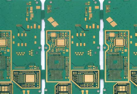
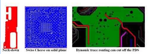
The latest high-density system-level chips use BGA or COB packaging, and the pin spacing is decreasing. The ball spacing has been as low as 0.6mm, and will continue to decrease, making it impossible to lead out the signal lines of packaged devices using traditional wiring tools. There are currently two methods to solve this problem: (1) lead the signal line from the lower layer through the via under the ball; (2) use ultra-fine wiring and free-angle wiring to find a lead channel in the ball grid array. For such high-density devices packaged in BGA or COB, the only feasible way is to use a wiring method with extremely small width and space. Only in this way can a high yield and reliability be guaranteed to meet high-speed design requirements.
2.3 Pad design of BGA package
With the development of device packaging technology, the relative size of device packages is getting smaller and smaller. TMS320C6000 series devices have up to 352 pins. Because the BGA pin spacing is dense and the via is very close to the pin, a large inductance will be generated. It is also harmful to high-speed signals, so when BGA is scattered, try to use smaller holes. There is a corresponding relationship between the size of the BGA pad and the BGA pin spacing, but it cannot be larger than the diameter of the BGA pin ball, which is usually about 1/10~1/5 of it. The vias and pads next to the BGA pads on the component surface must be plugged and covered with green oil. For BGA soldering, no other devices can appear within 2era around.
3 Conclusion
Digital signal processors are the core of signal processing. With the popularization of high-frequency devices, the density of printed circuit boards has increased, interference has increased, and the improvement of signal quality has been mentioned as the primary position of design. The PCB circuit board design of high-speed DSPs is a very complex design process. There are many factors that need to be considered when designing high-speed circuits, and these factors correspond to each other. For example, when high-speed devices are laid out, the position is close, which can reduce the delay, but may cause crosstalk and significant thermal effects; when routing, high-speed signals are wired in the inner layer as much as possible and there are fewer vias, which is also a contradiction. Therefore, in the design, it is necessary to comprehensively consider various favorable factors and make a comprehensive circuit design.
Only in this way can a high-quality PCB circuit board with strong anti-interference ability, stable performance and high real-time performance be designed