A preliminary study on the quantitative evaluation and application of PCB and PCBA process complexity
Background and objectives of the problem
As the precision and complexity of electronic information products become higher and higher, the design, production, and assembly of PCB and PCBA will bring new challenges and difficulties. In our work, due to the lack of quantitative evaluation of PCB and PCBA, we do not know how to distinguish between ordinary and complex PCB and PCBA designs, and what methods to use to deal with them.
Based on the above considerations, we refer to the existing practices in the industry and design a process complexity calculation formula for PCB and PCBA to solve this problem. On the other hand, in terms of engineering capabilities, we have done some targeted work to achieve such a goal of high quality and low cost.
Characteristics of high-complexity PCB
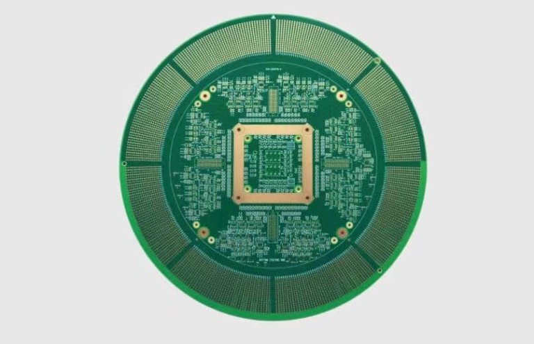
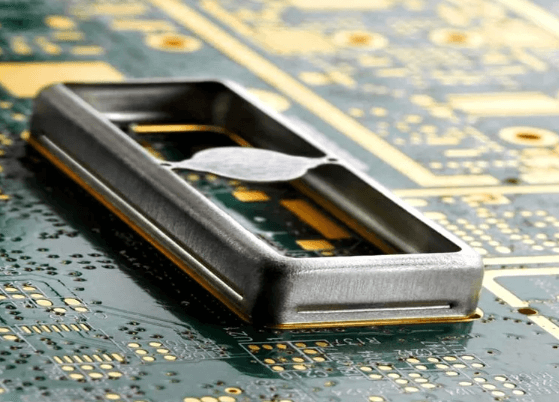
From our specific situation, high-complexity PCB has the following characteristics: large size, high layer count (more than 18 layers), 1+10+1 or even 1+16+1 HDI design, dense line width and line spacing (for example, 3/3, 3/4, 4/4), high hole thickness ratio (for example, more than 10:1, up to 13.5:1), and the use of some new surface treatment methods (such as chemical tin, chemical silver). We define such boards as high-complexity PCBs.
Quantification of PCB complexity
Then, we now give the definition of high-complexity PCB with four conditions: 1. Number of layers>18 (number of backplane layers>20); 2. Special processes such as HDI, mechanical buried blind holes, planar buried capacitance, back drilling, etc.; 3. Thickness ratio>10:1; 4. Appearance size close to the limit (minimum line width and line spacing <4mil; hole-to-line distance, including inner layer hole-to-line distance <10mil).
Characteristics of highly complex PCBA
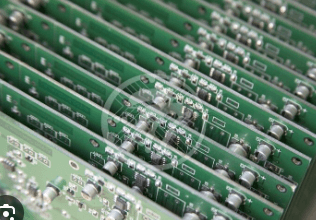
From our current situation, highly complex PCBA has the following characteristics: 1. A large number of components, up to 7,000-8,000; 2. Complex installation of structural parts; 3. Many area array components, even more than 60 area array components on a board, including CSP and BGA; 4. Double-sided layout; 5. Many resistor/capacitor matching components, and basically all 0402 or 0805 resistor/capacitor arrays; 6. Mixed SMT and THT.

PCBA Complexity Quantification Formula
We began to use the calculation formula of PCBA complexity index to consider these factors: 1. The number of components and solder joints; 2. Single-sided or double-sided layout; 3. Whether there are many mixed assemblies; 4. Solder joint density.
PCBA complexity index Ci = [(number of components + number of solder joints)/100] × S × M × D Where: S = number of sides of the PCB (for double-sided PCB, S = 1; for single-sided PCB, S = 1/2); M = process mixing degree (when the mixing degree is high, M = 1; when the mixing degree is low, M = 1/2); D = solder joint density, number of solder joints/square inch/100.
In addition to these factors, we also considered three other aspects:
1. Is an assembly process that has not been used before adopted?
2. Is a new board or auxiliary material used?
3. Are there any special assembly and assembly requirements? Points are added according to different weights from these three aspects.
A board with a complexity of less than 50 is a very simple board; a board with a complexity of 50 to 125 is a medium-complexity board; a board with a complexity of more than 125 is a high-complexity board. This definition can be adjusted according to your own situation. For example, we initially considered boards with a complexity greater than 80 to be very complex, but now with the improvement of capabilities, boards greater than 125 are considered relatively complex.
How to do high-complexity PCB and PCBA
By quantifying the complexity of PCB and PCBA, we have determined the PCB and PCBA that need to be focused on. Next, we need to work hard in two aspects: first, we need to do a good job of DFM for these PCB and PCBA during engineering design; second, we need to select suppliers with particularly strong engineering capabilities for these PCB and PCBA.
DFM of high-complexity PCB
When we do DFM for high-complexity PCB, we need to pay special attention to suppliers, materials, design, etc. For example, when designing PCB, the more layers there are, the lower the layer alignment accuracy will be. Therefore, we must be particularly careful when considering the aperture and the distance from the hole to the line.
Similarly, the hole width of the via should also be increased, because if the alignment is not accurate, the plate may be broken when drilling. Therefore, when designing a board with a large number of layers, we should appropriately increase the diameter of the inner hole plate. In addition, when considering the distance from the hole wall to the trace, we should pay special attention to the shrinkage problem of the high Tg board under thermal shock conditions.
When designing a high-complexity PCB, we must also be careful about the surface treatment.
From our current use, hot air leveling is not suitable for high-layer, large-size, and high-complexity boards. For ENIG, due to the small size of the pads of some fine-pitch and dense-pitch devices on high-complexity boards, the sensitivity to the black pad is greatly increased, so we now basically prohibit the use of ENIG surface treatment on high-complexity boards. For OSP, its adaptability to ICT testing needs to be considered.
DFM of High-complexity PCBA
For DFM of PCBA, the reflow soldering process route is preferred, and a small number of plug-ins, such as coaxial connectors and cable connectors, consider using through-hole reflow soldering. When there are a large number of plug-ins, centralized layout should be considered, and the process route of reflow soldering plus local wave soldering or selective wave soldering should be adopted to avoid manual soldering.
In addition, there should be corresponding requirements in various aspects such as the accuracy of graphic positioning, the impact of the diversity of device types on the assembly process and steel mesh design, the assembly capacity and maintenance of the equipment.
High-complexity PCBA assembly engineering capabilities of EMS manufacturers
For EMS manufacturers, the biggest problem we encounter is that EMS factories are not graded. There is no clear positioning from the perspective of personnel quality, equipment capabilities, and on-site process control capabilities to see whether they are suitable for high-complexity boards. We have also considered using different methods for different suppliers, such as using the method of fixed lines to solve the problem. However, can there be a clear requirement for improving the capabilities of the entire EMS factory and the capabilities of the personnel? Moreover, there is also a problem as to whether the capabilities of the line you set can be quantified. For example, for a board with a complexity of more than 200, what is the corresponding relationship between the technical capabilities of the corresponding personnel and the equipment capabilities? It is not clear now.
High-complexity PCBA assembly requirements
Whether it is an EMS manufacturer that provides assembly services or we do the processing ourselves, the control of high-complexity PCBA can be quantified into five aspects: people, machines, materials, methods, and environment.
People: Designate a special production line to process high-complexity boards, and formulate strict regulations and requirements for its equipment maintenance and operators, including training, examinations, job standards, etc.
Machine: There are strict control requirements for each device in each high-complexity product production line, including strict operating instructions, inspection requirements, etc. There are detailed regulations.
Material: Control and reduce tubular materials; The dimensional stability and solder end consistency of 0402 and 0201 micro devices should be good; pay attention to check whether the PCB has obvious deformation; The requirements for welding temperature of various types of device plating and solder ends should be basically the same; The size of the deformation of large-size connectors and module packages during reflow soldering should be within the allowable range, etc.
Method: For the control of process procedures, we now have a 30-page control procedure for the assembly of high-complexity PCBAs. Each step, including before boarding, replacement and addition of tin printing and tin paste, inspection of steel mesh before machine, and wiping paper and board washing water, has strict control requirements.
Environment: Strict control must be carried out in all aspects such as environmental conditions for material storage, anti-static management, moisture-sensitive device management, storage and turnover distribution of IC devices.
Application value of quantification methods for PCB and PCBA complexity
EMS manufacturers adopt different strategies in personnel composition, equipment configuration, and process control for PCBAs of different complexity to form layered processing capabilities to meet different customer needs; different processing costs can be required according to different PCBA complexities.
Through the operation of highly complex PCB and PCBA, the PCB production yield rate and PCBA assembly quality of ODM manufacturers have been significantly improved, the cost of rework and reliability risks have been reduced, and good economic benefits have been achieved. It can also be used to evaluate personnel input, process design strategy, and management model optimization.
At present, the quantitative standards of PCB and PCBA are applied by a few companies, but they have not been widely recognized and applied by the industry; and the projects involved in the quantitative standards are not perfect enough and need to be further optimized. It requires the participation of industry peers to form a unified quantitative standard for PCB and PCBA and promote it in the industry.