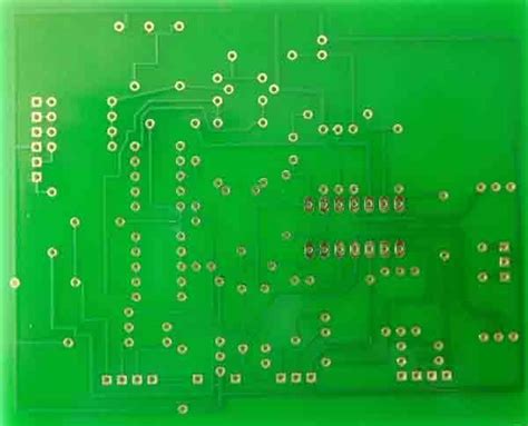
About the division of protel internal electrical layers
Protel99 has two types of electrical layers. Open a PCB design document and press the shortcut key L to display the layer setting window. The one on the left (SIGNAL LAYER) is the positive layer, including TOP LAYER, BOTTOM LAYER and MIDLAYER, and the one in the middle (INTERNAL PLANES) is the negative layer, namely INTERNAL LAYER. These two layers have completely different properties and usage methods.
Positive layers are generally used for pure circuits, including outer and inner layers.
Negative layers are mostly used for ground layers and power layers. Because the ground layers and power layers in multilayer boards are generally made of a whole piece of copper as a circuit (or as a division area for several larger blocks), if the MIDLAYER, i.e. the positive layer, is used for drawing, it must be implemented by copper plating, which will make the entire design data very large, which is not conducive to data communication and transmission, and will affect the design refresh speed. When using a negative film, you only need to generate a flower hole (THERMAL PAD) at the connection between the outer layer and the inner layer, which is very beneficial for design and data transmission.
Adding and deleting inner layers
In a design, sometimes you will encounter the situation of changing the board layer. For example, changing a more complex double-sided board to a four-layer board, or upgrading a four-layer board with higher signal requirements to a six-layer board, etc. At this time, you need to add an electrical layer, which can be done as follows:
DESIGN-LAYER STACK MANAGER, there is a schematic diagram of the current stacking structure on the left.
Click the layer above the position where you want to add a new layer, such as TOP, and then click ADD LAYER (positive film) or ADD PLANE (negative film) on the right to complete the addition of a new layer.
Note that if the newly added layer is a PLANE (negative film) layer, you must assign the corresponding network to this new layer (double-click the layer name)! There can only be one network assigned here (generally, a GND layer can be assigned). If you want to add a new network in this layer (such as a power layer), you must do an inner layer split in the subsequent operation to achieve it, so here you can first assign a network with a large number of connections.
If you click ADD LAYER, a MIDLAYER (positive film) will be added, and the application method is exactly the same as the outer layer line.
If you want to apply a mixed electrical layer, that is, a method with both routing and power ground copper surface, you must use the positive film layer generated by ADD LAYER to design (see below for the reason).
Split of inner electrical layer
If there is more than one set of power supplies in the design, you can use the inner layer split in the power layer to assign the power network. The command to be used here is:
PLACE-SPLIT PLANE, set the layer in the dialog box that appears, and specify the network to be assigned for this split at CONNECT TO NET, and then place the split area according to the copper plating method. After placement is completed, the holes with corresponding networks in this segmented area will automatically generate flower hole pads, which means that the electrical connection of the power layer is completed. This step can be repeated until all power supplies are allocated. When there are many networks to be allocated in the inner power layer, it is more troublesome to split the inner layer, and some skills are needed to complete it.
Here, we also need to pay attention to one issue: There are two electrical connection methods for large copper foils in PROTEL (excluding PLACE FILL), one is POLYGON PLANE, which is ordinary copper cladding. This command can only be applied to positive layers, including TOP/BOT/MIDLAYER, and the other is SPLIT PLANE, which is the inner power layer segmentation. This command can only be applied to negative layers, namely INTERNAL PLANE. It should be noted that the scope of use of these two commands should be distinguished.