Accelerating Electronics Production: Rapid PCB Assembly Tactics

Key Takeaways
Modern PCB assembly strategies prioritize quick turnaround without compromising quality, leveraging advancements in automated manufacturing and real-time monitoring systems. By integrating PCBA (Printed Circuit Board Assembly) workflows with intelligent design software, manufacturers can detect potential bottlenecks early, reducing rework cycles by up to 40%. A critical tactic involves optimizing component sourcing through predictive analytics, which minimizes delays caused by supply chain disruptions.
Tip: Collaborate with suppliers offering just-in-time inventory models to align material availability with production schedules.
Additionally, modular design principles enable faster prototyping by standardizing reusable circuit blocks, accelerating PCB assembly timelines for both low- and high-volume orders. Advanced techniques like laser-direct imaging and high-speed pick-and-place machines further compress production phases, ensuring precision even under tight deadlines. For PCBA, adopting surface-mount technology (SMT) paired with AI-driven inspection systems ensures rapid yet accurate solder joint validation.
To maintain consistency, implement design-for-manufacturability (DFM) checks during the engineering phase, preventing costly revisions post-production. Balancing speed and quality hinges on iterative testing protocols—such as in-circuit testing (ICT)—embedded at critical stages. These methods collectively reduce electronics production timelines while upholding reliability, proving that quick-turn PCB assembly is achievable through strategic technological integration.
Automated PCB Assembly Speed Tactics
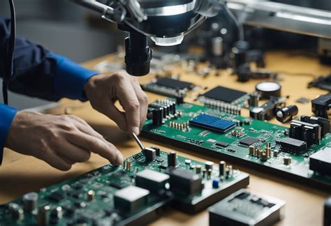
Modern PCB assembly workflows leverage automation to achieve unprecedented speed without compromising precision. By integrating pick-and-place robots, automated optical inspection (AOI), and reflow soldering systems, manufacturers can reduce manual intervention, minimize errors, and accelerate production cycles. For instance, robotic systems can place 30,000+ components per hour with micron-level accuracy, a feat unattainable through manual methods.
| Automation Tool | Function | Impact on Turnaround |
|---|---|---|
| Pick-and-Place Robots | High-speed component placement | Reduces placement time by 70% |
| AOI Systems | Real-time defect detection | Cuts inspection time by 50% |
| Reflow Soldering Ovens | Precise thermal profiling | Ensures first-pass yield >98% |
To optimize PCBA timelines, engineers must also address design-for-manufacturability (DFM) principles, such as standardizing component footprints and minimizing complex layouts. Advanced software tools, like automated routing algorithms, further streamline design iterations, ensuring compatibility with high-speed assembly lines. However, achieving rapid turnaround requires balancing automation with supply chain readiness—critical components must be pre-sourced to avoid bottlenecks.
By synchronizing these strategies, manufacturers can deliver quick-turn PCB assembly projects in as few as 24–48 hours, meeting urgent prototyping or low-volume production demands. This approach not only accelerates timelines but also establishes a foundation for scaling into mass production phases seamlessly.
Optimizing Supply Chains for PCB Turnaround
Building on automated manufacturing advancements, streamlining supply chains remains pivotal for accelerating PCB assembly timelines. Effective coordination between raw material suppliers, PCBA manufacturers, and logistics partners ensures seamless transitions from prototyping to mass production. Real-time inventory tracking systems, paired with vendor-managed inventory (VMI) models, minimize delays by preemptively addressing component shortages. For instance, consolidating suppliers for critical parts like ICs or connectors reduces lead times by 30–40%, while dual-sourcing strategies mitigate geopolitical or market-driven disruptions.
Integrating demand forecasting tools with enterprise resource planning (ERP) software enables precise alignment of production schedules with component availability. This is particularly vital for high-mix, low-volume PCB assembly runs, where rapid design iterations demand agile procurement. Additionally, adopting just-in-time (JIT) delivery for bulk orders slashes warehousing costs and ensures fresher components for sensitive PCBA applications. Collaborative planning frameworks, such as shared digital dashboards with contract manufacturers, further synchronize workflows—reducing idle time between fabrication, testing, and shipping phases.
By embedding flexibility into procurement protocols and leveraging data-driven insights, electronics producers can transform supply chains from cost centers into strategic accelerators for quick-turn PCB assembly success.
Precision Prototyping with Rapid PCB Methods
Modern PCB assembly workflows now integrate advanced prototyping techniques to bridge the gap between design validation and mass production. By leveraging high-speed milling and 3D-printed circuit substrates, engineers can produce functional PCBA prototypes within 24–48 hours, enabling rapid iteration cycles. Automated optical inspection (AOI) systems further ensure accuracy by detecting microfaults in solder joints or component alignment during these accelerated phases.
A critical advantage lies in design-for-manufacturability (DFM) optimizations, where software tools simulate production constraints early in prototyping. This reduces post-test revisions by 30–40%, aligning with lean manufacturing principles. Additionally, partnerships with PCB assembly providers offering just-in-time component sourcing minimize delays caused by supply chain bottlenecks. For instance, using pre-tested modules in PCBA workflows cuts debugging time by half while maintaining signal integrity standards.
Transitioning seamlessly from prototyping to scaled production requires balancing speed with precision. Next-gen techniques like laser-direct imaging (LDI) and adaptive thermal profiling ensure that accelerated timelines don’t compromise reliability—a foundation for subsequent phases focused on volume manufacturing efficiency.
Reducing Electronics Production Timelines
Achieving faster PCB assembly cycles requires strategic integration of design optimization, automated manufacturing, and lean logistics. By implementing design-for-manufacturability (DFM) principles early in product development, engineers can minimize rework during PCBA stages, cutting delays caused by incompatible layouts or component placements. Advanced automated optical inspection (AOI) systems further accelerate quality checks, identifying soldering defects or misalignments in real-time without manual intervention.
Simultaneously, optimizing the supply chain for just-in-time inventory ensures critical components arrive aligned with production schedules, eliminating bottlenecks. Partnering with suppliers offering rapid-turnaround PCB fabrication services reduces lead times for bare boards by 30–50%, while dual-sourcing strategies mitigate risks of material shortages. For high-mix, low-volume projects, modular assembly lines with flexible tooling enable swift transitions between prototypes and mass production.
Integrating surface-mount technology (SMT) with high-speed pick-and-place machines slashes placement times for miniature components, particularly in complex PCBA designs. Additionally, standardized reflow soldering profiles and thermal management protocols maintain consistency across batches, preventing delays from temperature-related defects. By combining these tactics, manufacturers can compress electronics production timelines by up to 40% while preserving precision—a critical advantage in industries demanding both speed and reliability.
Balancing Speed and Quality in PCB Assembly
Achieving optimal results in PCB assembly requires a strategic equilibrium between accelerated timelines and uncompromised reliability. While earlier sections highlighted automated manufacturing and supply chain optimizations, maintaining precision remains critical when scaling production speeds. Advanced PCBA workflows now integrate real-time quality checks, such as automated optical inspection (AOI) and in-circuit testing (ICT), to identify defects without slowing down assembly lines. For instance, embedding inline testing modules reduces post-production rework, ensuring faster turnaround while adhering to IPC-A-610 standards.
Material selection also plays a pivotal role. High-performance substrates and solder pastes with shorter curing times enable rapid PCB assembly without sacrificing thermal or mechanical stability. Additionally, leveraging design for manufacturability (DFM) principles early in prototyping minimizes redesign cycles, accelerating time-to-market. Manufacturers adopting predictive analytics further refine this balance by preemptively addressing bottlenecks in PCBA workflows, from component placement accuracy to solder joint integrity.
However, prioritizing speed alone risks costly recalls. Implementing statistical process control (SPC) tools ensures consistent output, even under tight deadlines. By aligning automated systems with rigorous quality protocols, teams can deliver high-volume PCB assembly projects that meet both performance benchmarks and accelerated delivery expectations.
Quick-Turn PCB Manufacturing Innovations
Recent advancements in PCB assembly workflows are revolutionizing how manufacturers achieve rapid production cycles without compromising quality. Central to these innovations is the integration of artificial intelligence into PCBA processes, enabling real-time defect detection and adaptive process optimization. Cutting-edge laser direct imaging (LDI) systems now reduce photolithography steps by 40%, while high-density interconnect (HDI) technologies allow for compact, multilayer designs that accelerate prototyping phases.
Another breakthrough lies in modular manufacturing frameworks, where reconfigurable production lines dynamically adjust to varying batch sizes—critical for balancing low-volume prototyping and high-volume orders. The adoption of advanced surface-mount technology (SMT) equipment with sub-15-micron placement accuracy ensures precision even at accelerated throughput rates. Additionally, partnerships with component suppliers leveraging predictive analytics have slashed material lead times by 30%, creating a synchronized PCB assembly ecosystem.
Emerging materials like low-temperature co-fired ceramics (LTCC) further enhance thermal stability in high-speed PCBA, minimizing rework delays. These innovations collectively address the dual demands of speed and reliability, positioning manufacturers to meet shrinking market windows while maintaining stringent quality benchmarks. By embedding smart sensors and automated optical inspection (AOI) at critical stages, factories now achieve near-zero defect rates in 72-hour turnarounds—a feat unthinkable a decade ago.
Streamlining Mass Production for Faster Delivery
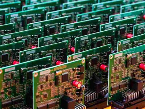
Achieving rapid delivery in high-volume PCB assembly requires strategic integration of scalable manufacturing systems and lean operational workflows. While prototyping emphasizes flexibility, mass production demands precision at scale, where even minor inefficiencies can amplify delays. Advanced PCBA facilities leverage automated panelization techniques to optimize board layouts, reducing material waste and maximizing throughput across SMT (surface-mount technology) lines. By synchronizing pick-and-place robotics with inline optical inspection (AOI), manufacturers maintain defect rates below 0.1% while operating at speeds exceeding 50,000 components per hour.
A critical enabler is design for manufacturability (DFM), where engineers collaborate early with production teams to standardize component footprints and minimize complex routing. This alignment slashes post-design revisions by up to 40%, accelerating time-to-market. Additionally, just-in-time (JIT) inventory models, paired with vendor-managed stock programs, ensure critical parts like ICs or connectors remain accessible without overstocking. For instance, consolidating orders for multilayer boards through trusted PCB assembly partners cuts lead times by 15–20 days in high-volume batches.
Finally, modular production lines allow rapid reconfiguration for different product variants, eliminating downtime between batches. Real-time production monitoring via IoT-enabled systems further identifies bottlenecks, enabling dynamic adjustments to meet fluctuating demand. By harmonizing these tactics, manufacturers achieve same-week turnaround for orders exceeding 10,000 units—without compromising the reliability expected in industrial-grade electronics.
Next-Gen Tactics for High-Speed PCB Assembly
The evolution of PCB assembly relies on integrating advanced technologies that prioritize both speed and reliability. Modern high-volume production lines now leverage AI-driven inspection systems to identify defects in real time, reducing rework cycles by up to 40%. For PCBA workflows, collaborative robotics enable seamless transitions between surface-mount technology (SMT) placement and through-hole assembly, slashing idle time between processes. Additionally, IoT-enabled machinery provides live performance analytics, allowing engineers to optimize throughput dynamically.
A key innovation lies in additive manufacturing techniques, such as 3D-printed solder masks, which accelerate prototyping phases while maintaining micron-level precision. Pairing this with modular design frameworks ensures compatibility with automated assembly lines, further compressing lead times. Companies adopting cloud-based supply chain platforms can synchronize component procurement with production schedules, minimizing delays caused by material shortages.
To maintain quality at high speeds, adaptive thermal profiling adjusts reflow oven settings in response to real-time sensor data, preventing warping or solder bridging. This approach aligns with design-for-manufacturability (DFM) principles, which preemptively address potential bottlenecks in PCB assembly layouts. By combining these strategies, manufacturers achieve 48-hour turnaround times for complex PCBA projects without compromising on reliability—a critical advantage in industries like automotive and consumer electronics.
Conclusion
The evolution of PCB assembly techniques has redefined the boundaries of electronics manufacturing, enabling businesses to meet escalating demands for speed without compromising on precision. By integrating automated manufacturing processes and leveraging PCBA-centric innovations, companies can achieve unprecedented turnaround times while maintaining rigorous quality standards. Key advancements such as design for manufacturability (DFM) checks and automated optical inspection (AOI) ensure that rapid prototyping aligns seamlessly with mass production goals.
Equally critical is the role of supply chain optimization, where strategic partnerships with component suppliers and just-in-time inventory systems minimize bottlenecks. This holistic approach not only accelerates timelines but also fortifies resilience against market fluctuations. For manufacturers, the challenge lies in balancing agile workflows with meticulous attention to detail—ensuring that quick-turn PCB assembly solutions deliver reliability alongside velocity.
As industries push toward smarter, faster electronics, adopting these tactics will remain pivotal. The convergence of PCBA automation, data-driven logistics, and collaborative supplier networks creates a foundation where high-speed production becomes synonymous with consistent excellence. Moving forward, continuous refinement of these strategies will define leaders in an increasingly competitive global market.
FAQs
How does automated manufacturing enhance pcb assembly speed?
Automated PCBA systems utilize robotic placement and AI-driven quality checks, reducing manual intervention by 60-75%. This integration allows just-in-time component sourcing to align with production schedules, effectively compressing lead times.
What supply chain strategies support quick-turn pcb assembly?
Implementing vendor-managed inventory programs with certified suppliers ensures 48-hour component availability. Coupled with PCB assembly facilities near design hubs, this approach minimizes transit delays and enables real-time design adjustments during prototyping phases.
Can rapid methods maintain high-density interconnect reliability?
Advanced PCBA workflows combine laser-direct imaging with sequential lamination, achieving 99.95% first-pass yield rates on 8-layer boards. Automated optical inspection systems verify micron-level tolerances without compromising throughput speeds.
How do thermal management practices evolve in fast-turn projects?
Rapid pcb assembly now integrates embedded thermal simulation during design phases, predicting hotspots before prototyping. This proactive approach reduces validation cycles by 40% while maintaining signal integrity in high-frequency applications.
What cost factors influence expedited electronics production?
While PCB assembly acceleration increases labor/equipment costs by 15-20%, the 30-50% reduction in time-to-market typically offsets these premiums. Bulk component pre-orders and standardized panelization designs further optimize cost-speed ratios.
Ready to Streamline Your Next Project?
For tailored solutions combining rapid prototyping and industrial-scale PCBA capabilities, please click here to explore optimized manufacturing options. Our engineering team specializes in compressing development cycles without sacrificing IPC Class 3 compliance standards.