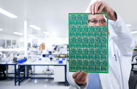
Achieving Efficient Automated PCB Routing Design
Although current EDA tools are powerful,PCB design remains challenging as PCB dimensions shrink and device density increases.How can we achieve high PCB routing yields and shorten design time?This article introduces design techniques and key points for PCB planning layout,and routing.While PCB design time is shrinking,shrinking board space,increasing device density,extremely stringent layout rules,and large component are making the designer’s work even more challenging.To address these design challenges and speed product time to market,many manufacturers are turning to dedicated EDA tool for PCB design.However,dedicated EDA tools don’t produce ideal result,don’t achieve 100% routing yields,and are often cluttered,requiring significant time to complete.
There are many popular EDA tools on the market,but aside from terminology and function key placement,they are largely similar.How can we best utilize these tools for PCB design?Carefully analyzing the design and configuring the tool before beginning routing will ensure that the design meet your requirements.The following is a general design process and steps.
1.Determine the Number of PCB Layers
The board size and number of routing layers must be determined early in the design process.If the design calls for high-density ball grid array(BGA)components,the minimum number of routing layers required to route these component must be considered.The number of routing layers and the stack-up method directly impact trace routing and impedance.Board size helps determine the stack-up method and trace width to achieve the desired design results.
For many years,it was believed that fewer layers meant lower costs,but many other factors influence PCB manufacturing costs.In recent years,the cost difference between multilayer board has significantly narrowed.It’s best to use a large number of circuit layers and distribute the copper evenly at the beginning of the design process to avoid discovering near the end that a small number of signals do not meet the defined rules and space requirements,forcing the addition of new layers.Careful planing before the design phase can save significant routing headaches.
2.Design Rules and Constraints
Automatic routing tools don’t inherently know what to do .To complete the routing task,they must work within the correct rules and constrains.Different signal lines have different routing requirements.All signal lines with special requirement.All signal lines with special requirement must be categorized,and categorization varies from design to design.Each signal class should have a priority,with higher priorities imposing stricter rules.These rules include trace width,maximum number of vias,parallelism,signal line interactions,and layer restrictions.These rules significantly.impact routing tool performance.Careful consideration of design requirements is a crucial step in succesful routing.
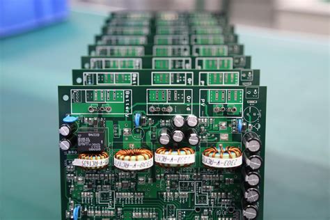
3.Component layout
To optimize the assembly process,Design for Manufacturability(DFM) rules impose constrains on component placement.If the assembly department allows component movement,the circuit can be optimized to facilitate automatic routing.The defined rules and constrain influence the layout design.
During layout,routing channels and via areas must be considered.While these channels and areas are obvious to the designer,automatic routing tools only consider one signal at a time.By setting routing constraints and specifying the layers on which signal lines can be routed,the routing tool can ensure that the routing is performed as the designer intended.
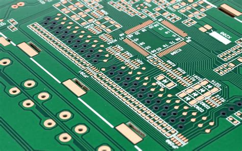
4.Fan-out Design
During the fan-out design phase,to enable automated routing tools to connect component pins,each pin of a surface-mount device should have a least one via.This allows for inner-layer connections,in-circuit testing(ICT),and circuit reprocessing when more connections are needed.
To maximize automated routing tool efficiency, it is crucial to use the largest possible via size and trace spacing;ideally,a spacing of 50 mils is ideal.Via types that maximize the number of routing paths should be used.When designing fan-out,consider in-circuit testing.Test fixtures can be expensive and are often ordered near the start of full production.Adding nodes to achieve 100% testability at this point is too late.
With careful consideration and foresight in-circuit testing can be designed early in the design process and implemented later in the production process.via fan-out types are determined based on routing paths and incircuit testing.Power and grounding considerations also influence routing and fan-out design.To reduce the inductance of the filter capacitor connection wires,vias should be placed as close as possible to the surface-mount device pins. Manual routing can be used if necessary.This may affect the originally planned routing path and may even lead to a reconsideration of the via type.Therefore,it is important to consider the relationship between via and pin inductance and prioritize via specifications.
5.Manual Routing and Handing of Critical Signals
Although this article primarily discusses automatic routing,manual routing is and will continue to be an important process in PCB design.Manual routing facilitates the routing work of automatic routing tools.
Regardless of the number of critical signals these signals should be routed first,either manually or in conjunction with automatic routing tools. Critical signals often require careful circuit design to achieve the desired performance.After routing is completed,the routing of these signals should be checked by the relevant engineering staff,which is a relatively easy process.Once the check is passed,these wires are fixed,and automatic routing can begin for the remaining signals.
6.Autorouting
When routing critical signals,it’s important to consider controlling certain electrical parameters,such as minimizing distributed inductance and EMC.The same applies to routing other signals.All EDA vendors provide methods to control these parameters.Understanding the autorouting tool’s input parameters and their impact on routing can help ensure the quality of autorouting.
General rules should be applied to autorouting signals.By setting constraints and keepout zones to limit the layers and number of vias used for a given signal,the routing tool can automatically route according to the engineer’s design.If the autorouting tool doesn’t set limits on the layers and number of vias used,it will use every layer and generate many vias.
After setting constraints and applying the created rules,autorouting should achieve result colse to your expectation.Of course,some cleanup may be required,and you should also ensure space for other signals and nets.After completing a portion of the design,fix it to prevent it from being affected by subsequent routing.
Use the same steps to route the remaining signals.The number of routing times depends on the complexity of the circuit and the number of general rules you define.After completing each signal type,the routing constrains for the remaining nets are reduced.However,this means that many signals will require manual routing.Today’s autorouting tools are very powerful and can typically complete 100% of routing.However,when the autorouting tool doesn’t complete all signal routing,the remaining signal will need to be routed manually.
7.Key points for autorouting design include:
7.1 Slightly change the setting to experiment with various routing paths;
7.2 Maintaining the same basic rules,experiment with different routing layers,trace and space widths,line widths,and different types of vias(such as blind and buried via)to observe how these factors affect the design results:
7.3 Allow the routing tool to process the default nets as needed;
8 Routing Management
If your EDA tool lists signal routing lengths examining this data may reveal that some signals with few constraints have very long routing lengths.This problem is relatively easy to address.Manual editing can shorten signal routing lengths and reduce the number of vias. During the review process,you need to determine which routing patterns are appropriate and which are inappropriate.Like manual routing,automated routing also allows for review and editing.
9.PCB Appearance
Previously,designers often focused on the visual appearance of the PCB.This is no longer this case.While automated designs may not be as aesthetically pleasing as manually designed ones,they will still meet the specified electronic performance requirements,ensuring the integrity of the design.