Acquisition and application of electromagnetic information of PCB board
The traditional tools for debugging PCB include: time domain oscilloscope, TDR (time domain reflectometry) oscilloscope, logic analyzer, and frequency domain spectrum analyzer, but these means cannot give a data reflecting the overall information of PCB board. PCB board is also called printed circuit board, printed wiring board, abbreviated as printed board, English abbreviation PCB (printed circuit board) or PWB (printed wiring board), with insulating board as base material, cut into a certain size, with at least one conductive pattern attached to it, and holes (such as component holes, fastening holes, metallized holes, etc.) are arranged to replace the chassis of electronic components in the past, and realize the interconnection between electronic components. Because this board is made by electronic printing, it is called “printed” circuit board. It is not accurate to call “printed circuit board” “printed circuit” because there are no “printed components” but only wiring on the printed board.
The Emscan electromagnetic compatibility scanning system uses advanced array antenna technology and electronic switching technology to measure the current of PCB at high speed. The key to Emscan is the use of advanced array antenna to measure the near-field radiation of the working PCB placed on the scanner. This antenna array consists of 40 x 32 (1280) small H-field probes, which are embedded in an 8-layer circuit board, on which a protective layer is added to place the PCB under test. The results of the spectrum scan can give us a general understanding of the spectrum generated by the EUT: how many frequency components there are and what is the approximate amplitude of each frequency component.
Full-band scanning
The design of the PCB board is based on the circuit schematic to achieve the functions required by the circuit designer. The design of the printed circuit board mainly refers to the layout design, which needs to consider various factors such as the layout of external connections, the optimized layout of internal electronic components, the optimized layout of metal connections and through holes, electromagnetic protection, and heat dissipation. The layout design can save production costs and achieve good circuit performance and heat dissipation performance. Simple layout design can be implemented manually, and complex layout design needs to be implemented with the help of computer-aided design.
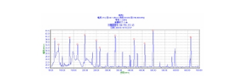
When performing the spectrum/space scanning function, place the working PCB on the scanner, and the PCB is divided into 7.6mm×7.6mm small grids by the scanner grid (each small grid contains an H-field probe). After performing a full-band scan of each probe (the frequency range can be from 10kHz to 3GHz), Emscan finally gives two pictures, namely the synthetic spectrum map (Figure 1) and the synthetic space map (Figure 2).
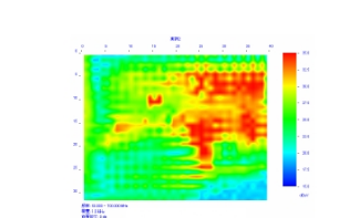
The spectrum/space scanning obtains all the spectrum data of each probe in the entire scanning area. After performing the spectrum/space scanning, the electromagnetic radiation information of all frequencies in all spatial positions can be obtained. You can imagine the spectrum/space scanning data in Figures 1 and 2 as a pile of space scanning data, or as a pile of spectrum scanning data. You can:
- View the spatial distribution diagram of the specified frequency point (one or more frequencies) as shown in Figure 3, just like viewing the spatial scan results.
- View the spectrum diagram of the specified physical location point (one or more grids) as shown in Figure 4, just like viewing the spectrum scan results.
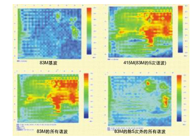
The various spatial distribution diagrams in Figure 3 are the spatial abdomen diagrams of the frequency point by specifying the frequency point. It is obtained by specifying the frequency point with × in the spectrum diagram above the figure. You can specify a frequency point to view the spatial distribution of each frequency point, or you can specify multiple frequency points, such as specifying all harmonic points of 83M to view the total spectrum diagram.
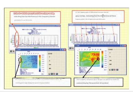
In the spectrum diagram of Figure 4, the gray part is the total spectrum diagram, and the blue part is the spectrum diagram of the specified position. The location of the interference source is found by specifying the physical location on the PCB with ×, and comparing the spectrum diagram (blue) and the total spectrum diagram (gray) generated at the location. As can be seen from Figure 4, this method can quickly find the location of the interference source for both broadband interference and narrowband interference.
Quickly locate the source of electromagnetic interference
A spectrum analyzer is an instrument for studying the spectrum structure of electrical signals. It is used to measure signal parameters such as signal distortion, modulation, spectral purity, frequency stability and intermodulation distortion. It can be used to measure certain parameters of circuit systems such as amplifiers and filters. It is a multi-purpose electronic measuring instrument. It can also be called a frequency domain oscilloscope, tracking oscilloscope, analytical oscilloscope, harmonic analyzer, frequency characteristic analyzer or Fourier analyzer. Modern spectrum analyzers can display the analysis results in analog or digital form, and can analyze electrical signals in all radio frequency bands from very low frequency below 1 Hz to submillimeter wave bands.
Using a spectrum analyzer and a single near-field probe, it is also possible to locate the “interference source”. Here, the “fire extinguishing” method is used as an analogy. The far-field test (EMC standard test) can be likened to “detecting a fire”. If a frequency point exceeds the limit value, it is considered to be “discovering a fire”. The traditional “spectrum analyzer + single probe” solution is generally used by EMI engineers to detect “where the flames are coming from the chassis”. After detecting the flames, the general EMI suppression method is to use shielding and filtering to cover the “flames” inside the product. EMSCAN allows us to detect the source of the interference source – the “fire”, and also see the “fire”, that is, the propagation path of the interference source.
It can be clearly seen from Figure 4 that using “complete electromagnetic information” to locate the electromagnetic interference source is very convenient, which can not only solve the problem of narrowband electromagnetic interference, but also the problem of broadband electromagnetic interference.
The general method is as follows:
(1) Check the spatial distribution of the fundamental wave and find the physical position of the amplitude on the spatial distribution diagram of the fundamental wave. For broadband interference, specify a frequency in the middle of the broadband interference (for example, for a 60MHz-80MHz broadband interference, we can specify 70MHz), check the spatial distribution of the frequency point, and find the physical position of the amplitude.
(2) Specify the location and look at the spectrum diagram of the location. Check whether the amplitude of each harmonic point at the location coincides with the total spectrum diagram. If so, it means that the specified location is the place where these interferences are generated. For broadband interference, check whether the location is the location of the entire broadband interference.
(3) In many cases, not all harmonics are generated at one location. Sometimes even harmonics and odd harmonics are generated at different locations, or it is possible that each harmonic component is generated at different locations. In this case, you can find the location with strong radiation by looking at the spatial distribution of the frequency points you are concerned about.
(4) Taking measures at the location with strong radiation is undoubtedly effective in solving EMI/EMC problems.
This EMI troubleshooting method that can truly track the “source” and propagation path allows engineers to eliminate EMI problems at a low cost and fast speed. In the actual measurement of a communication device, the radiation interference radiates from the telephone line cable. After using EMSCAN to perform the above tracking scan, several more filter capacitors were finally installed on the processor board, solving the EMI problem that the engineer could not solve before.
Quickly locate the circuit fault position
With the increasing complexity of PCB, the difficulty and workload of debugging are also increasing. Using an oscilloscope or logic analyzer, only one or a limited number of signal lines can be observed at the same time, while there may be thousands of signal lines on the current PCB. Engineers can only rely on experience or luck to find the problem.
If we have the “complete electromagnetic information” of the normal board and the faulty board, by comparing the data of the two, we can find the abnormal spectrum, and then use the “interference source positioning technology” to find the location of the abnormal spectrum, and then we can quickly find the location and cause of the fault.
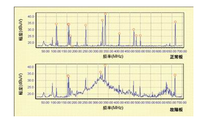
Figure 5 is the spectrum diagram of the normal board and the faulty board. By comparing, it is easy to find that there is an abnormal broadband interference on the faulty board.
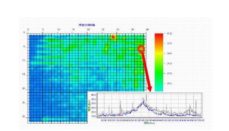
Then find the location of this “abnormal spectrum” on the spatial distribution diagram of the faulty board, as shown in Figure 6. In this way, the fault location is located at a grid (7.6mm×7.6mm) position, and the problem can be quickly diagnosed.
Application of evaluating PCB design quality
A good PCB requires careful design by engineers, and the issues to be considered include:
(1) Reasonable stacking design
Especially the arrangement of ground plane and power plane, as well as the design of the layer where sensitive signal lines and signal lines that generate a lot of radiation are located. There is also the division of ground plane and power plane, and the routing of signal lines across the divided area.
(2) Keep the signal line impedance as continuous as possible
As few vias as possible; as few right-angle routing as possible; and as small current return area as possible can generate fewer harmonics and lower radiation intensity.
(3) Good power supply filtering
The reasonable type, capacitance, quantity, and placement of filter capacitors, as well as the reasonable stacking arrangement of ground plane and power plane, can ensure that electromagnetic interference is controlled in the smallest possible area.
(4) Ensure the integrity of the ground plane as much as possible
As few vias as possible; reasonable via safety spacing; reasonable device layout; reasonable via arrangement to ensure the integrity of the ground plane. On the contrary, dense vias and excessive via safety spacing, or unreasonable device layout, will seriously affect the integrity of the ground plane and the power plane, thereby generating a large amount of inductive crosstalk and common mode radiation, and will make the circuit more sensitive to external interference.
(5) Find a compromise between signal integrity and electromagnetic compatibility
On the premise of ensuring the normal function of the equipment, increase the rising and falling edge time of the signal as much as possible, and reduce the amplitude and number of harmonics of the electromagnetic radiation generated by the signal. For example, it is necessary to select a suitable damping resistor, a suitable filtering method, etc.
Previously, the complete electromagnetic field information generated by the PCB can be used to scientifically evaluate the PCB design quality. Using the complete electromagnetic information of the PCB, the design quality of the PCB can be evaluated from the following four aspects: 1. The number of frequency points: that is, the number of harmonics. 2. Transient interference: unstable electromagnetic interference. 3. Radiation intensity: the amplitude of electromagnetic interference at each frequency point. 4. Distribution area: the size of the distribution area of electromagnetic interference at each frequency point on the PCB.
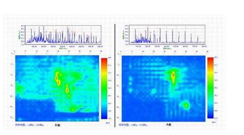
In the following example, board A is an improvement of board B. The schematic diagrams and layout of the main components of the two boards are exactly the same. The results of the spectrum/spatial scan of the two boards are shown in Figure 7:
From the spectrum diagram in Figure 7, it can be seen that the quality of board A is obviously better than that of board B, because:
- The number of frequency points of board A is obviously less than that of board B;
- The amplitude of most frequency points of board A is smaller than that of board B;
- The transient interference of board A (frequency points not marked) is less than that of board B.
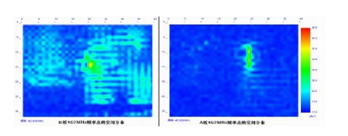
From the spatial diagram, it can be seen that the total electromagnetic interference distribution area of board A is much smaller than that of board B. Let’s take a look at the electromagnetic interference distribution at a certain frequency point. From the electromagnetic interference distribution of the frequency point of 462MHz shown in Figure 8, the amplitude of board A is small and the area is very small. The amplitude of board B is large and the distribution area is particularly wide.
Summary of this article
Complete electromagnetic information of PCB can give us a very intuitive understanding of the overall PCB, which not only helps engineers solve EMI/EMC problems, but also helps engineers debug PCB and continuously improve the design quality of PCB. Similarly, EMSCAN has many applications, such as helping engineers solve electromagnetic sensitivity problems, etc.


