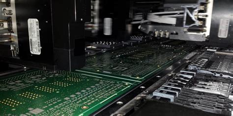
Additive PCB Manufacturing: Rapid Prototyping Complex Electronics
Key Takeaways
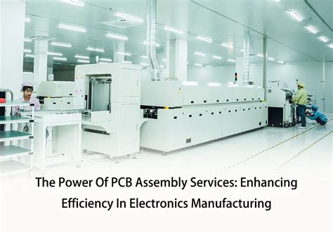
When exploring PCB manufacturing methods, you’ll find additive techniques offer distinct advantages for modern electronics development. Unlike traditional subtractive processes, which carve away copper to create circuits, additive manufacturing builds conductive traces layer by layer. This approach slashes material waste by up to 70%, directly addressing concerns around PCB manufacturing cost for low-volume projects.
For PCB manufacturing companies, this method enables rapid iteration of multi-layer designs without costly tooling changes. You can prototype complex circuitry in days rather than weeks, making it ideal for startups or R&D teams testing advanced concepts. The precision of additive processes also supports high-density interconnects, critical for miniaturized devices like wearables or IoT sensors.
Here’s a quick comparison of key factors:
| Aspect | Additive PCB | Traditional PCB |
|---|---|---|
| Setup Time | Hours | Days |
| Material Waste | <10% | 30-50% |
| Scalability | Low-Volume Optimized | Mass Production |
While additive methods aren’t replacing conventional PCB manufacturing business models entirely, they complement them by filling gaps in speed and flexibility. For projects requiring quick turns or intricate geometries, additive solutions often outperform subtractive alternatives. By integrating these techniques, you reduce time-to-market and unlock new possibilities in electronics design.
Rapid Prototyping with Additive PCB Tech
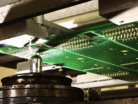
When developing complex electronics, additive PCB manufacturing accelerates prototyping cycles by enabling direct printing of conductive traces and dielectric layers. Unlike subtractive methods that require etching away excess material, this process builds circuits layer-by-layer, reducing waste and allowing for iterative design adjustments in days instead of weeks. Functional prototypes with multi-layer architectures can now be tested faster, helping you validate performance before committing to mass production.
"Additive methods cut tooling lead times by 60–80%, making them ideal for validating high-frequency or embedded component designs."
For PCB manufacturing companies, this flexibility addresses the growing demand for customized, low-volume solutions. Traditional PCB manufacturing cost structures often penalize small batches, but additive systems eliminate costly photomasks and molds. You’ll find this particularly advantageous when prototyping high-density interconnects or hybrid rigid-flex boards. By integrating additive workflows, PCB manufacturing businesses can offer clients faster turnaround without sacrificing precision—critical for industries like medical devices or aerospace.
Transitioning to additive processes does require reevaluating material choices and printer capabilities. However, the ability to rapidly test thermal management solutions or signal integrity in 3D-printed boards often outweighs initial setup investments. As geometries shrink and component integration intensifies, additive PCB manufacturing bridges the gap between concept and functional prototype more efficiently than ever.
Multi-Layer Electronics via Additive Methods
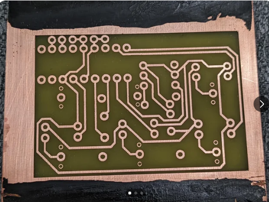
When designing multi-layer electronics, additive PCB manufacturing methods offer unique advantages for creating intricate, stacked circuitry. Unlike traditional subtractive processes that remove copper to form traces, additive techniques precisely deposit conductive materials layer by layer. This approach eliminates the need for mechanical drilling, enabling seamless vertical interconnects between layers while maintaining signal integrity.
For PCB manufacturing companies, this method reduces PCB manufacturing cost by minimizing material waste and avoiding costly tooling changes. You can prototype multi-layer boards with 8+ conductive layers in days rather than weeks—a critical advantage when testing high-frequency or miniaturized designs. The ability to embed passive components directly into dielectric layers further simplifies assembly, reducing dependency on secondary processes.
In low-volume production runs, additive manufacturing supports hybrid designs where flexible and rigid sections coexist within the same board. This flexibility is invaluable for applications like medical devices or aerospace systems, where space constraints demand compact, high-density layouts. By integrating additive workflows, PCB manufacturing businesses can address niche markets requiring rapid iterations without compromising precision.
Transitioning to additive methods doesn’t replace conventional manufacturing but complements it, offering a strategic path to handle complex geometries that traditional techniques struggle to execute cost-effectively.
Low-Volume PCB Production Using AME
When you need functional prototypes or specialized electronic components in limited quantities, traditional PCB manufacturing methods often struggle to justify their setup costs and lead times. Additive manufacturing electronics (AME) eliminates these barriers by enabling tooling-free production, allowing PCB manufacturing companies to bypass expensive molds, etching processes, and material waste. This approach is ideal for low-volume runs—think dozens to hundreds of units—where minimizing PCB manufacturing cost while maintaining precision is critical.
AME systems layer conductive and dielectric materials directly onto substrates, creating circuits without subtractive steps. This design flexibility lets you iterate complex geometries rapidly, whether you’re testing a new IoT sensor or refining a medical device’s circuitry. For startups or R&D teams, this means faster validation cycles and reduced financial risk. Even established PCB manufacturing business models benefit, as AME complements traditional workflows for niche projects requiring quick turnaround.
By integrating AME, you eliminate minimum order quantities (MOQs) tied to conventional fabrication. Instead, you pay per unit, aligning expenses with actual demand. This scalability ensures low-volume production remains economically viable, especially for applications like aerospace or automotive subsystems where customization trumps mass production. With AME, your team can pivot designs faster, respond to client feedback in real time, and maintain tighter control over intellectual property—advantages that solidify its role in modern electronics development.
High-Precision Additive PCB Applications
When developing specialized electronics requiring micron-level accuracy, additive PCB manufacturing methods excel in creating intricate circuits that traditional etching struggles to replicate. This precision is critical for applications like medical implants, aerospace sensors, or RF devices, where substrate conformity and trace density directly impact performance. By eliminating photomasks and chemical baths, additive processes reduce PCB manufacturing cost for low-volume runs, allowing you to iterate designs without compromising on quality.
Leading PCB manufacturing companies now integrate additive systems to produce hybrid boards combining rigid and flexible layers—ideal for wearable tech or IoT devices needing 3D-compatible circuitry. The technology’s ability to deposit conductive inks with ±10μm accuracy also minimizes material waste, a key advantage for startups managing tight budgets in the PCB manufacturing business. While subtractive methods dominate mass production, additive techniques unlock new possibilities for prototyping high-frequency circuits or embedded components, ensuring your projects meet exacting standards without delays.
Additive vs Traditional PCB Manufacturing
When choosing between additive PCB manufacturing and traditional methods, you’ll notice distinct trade-offs in flexibility, speed, and scalability. Traditional processes, like subtractive etching, excel in high-volume production by chemically removing excess copper from pre-coated boards—ideal for standardized designs. However, they often involve higher PCB manufacturing cost due to tooling setups and material waste. In contrast, additive techniques build circuits layer-by-layer using conductive inks or pastes, eliminating wasteful steps and enabling rapid design iterations. This makes additive methods particularly advantageous for low-volume PCB manufacturing business needs, where prototyping complex, multi-layer designs demands agility.
While traditional PCB manufacturing companies dominate mass production, additive systems reduce lead times from weeks to days for prototypes. You’ll also avoid minimum order quantities, which lowers upfront investments. Yet, additive’s precision currently lags behind traditional methods for ultra-fine traces, making hybrid approaches common for balancing cost-efficiency and performance. For projects requiring quick validation of intricate layouts, additive workflows complement—rather than replace—conventional systems, reshaping how engineers approach PCB manufacturing in evolving markets.
Complex Circuitry Design with Additive PCBs
When designing intricate electronic systems, additive PCB manufacturing unlocks possibilities that traditional methods struggle to match. By leveraging layer-by-layer deposition, you can achieve geometries with high-precision interconnects, embedded passive components, and three-dimensional structures—all critical for advanced applications like IoT sensors or aerospace systems. Unlike subtractive processes, which remove material to create circuits, additive techniques build conductive traces directly, reducing waste and enabling finer resolutions (down to 25µm).
For PCB manufacturing companies, this approach simplifies prototyping multi-layer designs without costly tooling changes. You can iterate rapidly on complex layouts, testing functional density or signal integrity before committing to mass production. This flexibility is particularly valuable in low-volume scenarios, where PCB manufacturing cost often hinges on setup expenses. Additionally, additive methods support hybrid designs—combining rigid and flexible substrates—to meet demands for compact, lightweight devices.
While traditional PCB manufacturing business models prioritize scale, additive technologies shift the focus to customization. Engineers gain freedom to integrate thermal management features or antenna arrays directly into the board’s architecture, bypassing post-assembly modifications. However, balancing material properties (like conductivity and durability) remains key—a consideration that underscores the importance of partnering with specialists in additive PCB manufacturing.
Benefits of Additive Manufacturing in Electronics
When developing complex electronic systems, PCB manufacturing through additive methods offers distinct advantages over traditional processes. By eliminating the need for subtractive etching, you reduce material waste by up to 70%, directly lowering PCB manufacturing cost for low-volume projects. This approach enables rapid design iterations, allowing you to test intricate circuitry in days rather than weeks—a critical edge for startups or R&D teams.
For PCB manufacturing companies, additive techniques unlock the ability to produce multi-layer boards with embedded components, minimizing assembly steps and improving reliability. The precision of laser-driven deposition ensures tolerances under 25 microns, ideal for high-frequency or miniaturized devices. Additionally, since tooling isn’t required, you avoid upfront investments in molds or masks, making it easier to scale a PCB manufacturing business without compromising quality.
Transitioning to additive workflows also future-proofs your operations. As demand grows for customized IoT or wearable electronics, the flexibility to prototype and produce on-demand positions your projects ahead of competitors relying solely on conventional methods. This shift doesn’t replace traditional manufacturing but complements it, creating hybrid strategies that balance speed, cost, and complexity.
Conclusion
When evaluating PCB manufacturing strategies, additive methods offer distinct advantages for prototyping and low-volume production. By enabling rapid iteration of complex designs, this approach reduces development cycles and allows PCB manufacturing companies to test intricate layouts without the upfront costs of traditional tooling. While conventional processes remain efficient for mass production, additive techniques excel in scenarios requiring high precision and flexibility—particularly for multi-layer electronics or specialized applications.
For businesses balancing PCB manufacturing cost with performance demands, hybrid workflows that combine additive and subtractive methods often deliver optimal results. This strategy minimizes material waste while maintaining the geometric freedom needed for advanced circuitry. As you explore options for your PCB manufacturing business, consider how additive technologies can complement existing capabilities, ensuring scalability without compromising on innovation. The key lies in aligning your production model with the specific demands of each project, leveraging the strengths of both approaches to stay competitive in evolving markets.
FAQs
How does additive manufacturing differ from traditional PCB manufacturing?
Additive methods build circuits layer-by-layer using specialized materials, eliminating the need for etching or drilling. This reduces PCB manufacturing cost for low-volume runs while enabling complex geometries that traditional PCB manufacturing companies struggle to achieve.
What types of electronics benefit most from additive PCB processes?
Applications requiring high-density interconnects or customized form factors—such as medical devices or IoT sensors—see significant advantages. Additive workflows let you prototype multi-layer designs faster than conventional PCB manufacturing business workflows.
Is additive manufacturing suitable for high-volume production?
While ideal for prototyping and small batches, current speed limitations make traditional methods more cost-effective at scale. However, hybrid approaches allow PCB manufacturing firms to combine additive precision with subtractive efficiency.
How do material choices impact additive PCB performance?
Conductive inks and substrates determine thermal stability and conductivity. Reputable PCB manufacturing companies optimize material stacks for your application, balancing durability and signal integrity without overengineering costs.
Ready to Explore Additive PCB Solutions?
For tailored guidance on integrating additive techniques into your project, please click here to consult with industry experts.