Additive PCB Techniques Reshaping Modern Electronics Manufacturing

Key Takeaways
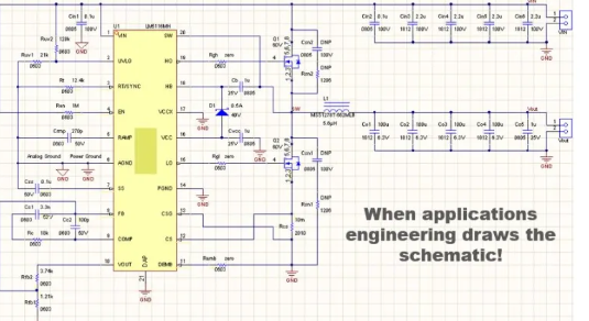
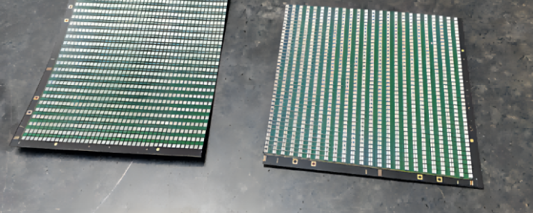
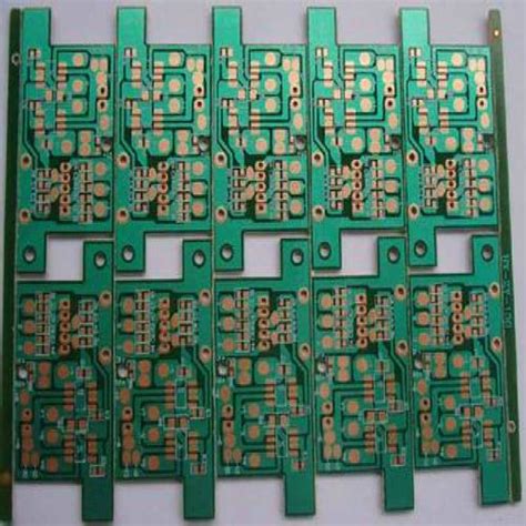
When exploring additive PCB techniques, you’ll discover how they redefine PCB manufacturing by eliminating traditional subtractive processes. Unlike conventional methods that rely on etching away excess material, additive approaches build circuits layer-by-layer, reducing waste and slashing PCB manufacturing cost by up to 30%. For PCB manufacturing companies, this means faster prototyping and the ability to produce complex geometries that were once impractical.
A critical advantage lies in scalability. Whether you’re running a small PCB manufacturing business or managing large-scale production, additive methods adapt seamlessly. For example, sustainable production practices become achievable through material efficiency, aligning with global eco-conscious trends.
| Factor | Traditional PCB | Additive PCB |
|---|---|---|
| Material Waste | High (~60%) | Low (<10%) |
| Design Flexibility | Limited | High |
| Time-to-Market | 2-3 weeks | 5-7 days |
By integrating additive tech, you gain precision in creating high-density interconnects while avoiding costly errors. This shift not only streamlines workflows but also empowers innovation—key for staying competitive in a rapidly evolving industry.
Additive PCB Manufacturing Benefits
Adopting additive PCB manufacturing techniques allows you to rethink how circuits are built, offering advantages that traditional methods struggle to match. Unlike subtractive processes that remove excess copper, additive techniques deposit conductive materials only where needed, reducing pcb manufacturing cost by minimizing waste. This precision translates to faster production cycles, enabling pcb manufacturing companies to meet tight deadlines without compromising quality.
“Switching to additive methods can cut material usage by up to 70%, making it a strategic move for businesses aiming to balance efficiency and sustainability.”
For pcb manufacturing business models, additive processes unlock design flexibility. You can create intricate, high-density circuits that support advanced applications like wearables or IoT devices. This scalability also lowers entry barriers for smaller enterprises, as additive systems require fewer upfront tooling investments. Additionally, the reduced chemical usage aligns with eco-conscious trends, appealing to clients prioritizing green electronics.
By integrating additive workflows, you not only streamline pcb manufacturing but also future-proof operations against rising material costs and regulatory shifts. The ability to prototype rapidly and tweak designs on-demand ensures your business stays agile in a competitive market.
Sustainable Electronics Production Methods
When evaluating PCB manufacturing processes, you’ll notice traditional subtractive methods often generate significant waste through excessive material etching. Additive techniques, however, build circuits layer by layer, minimizing raw material consumption by up to 70%. This precision reduces energy demands during production, aligning with global sustainability goals while lowering PCB manufacturing cost for companies.
By adopting additive workflows, PCB manufacturing companies can eliminate toxic chemical byproducts common in conventional processes. This shift not only supports compliance with environmental regulations but also enhances brand reputation among eco-conscious clients. For instance, businesses leveraging these methods report 30-40% reductions in hazardous waste disposal expenses—a critical advantage in scaling a PCB manufacturing business.
Moreover, additive processes enable the use of recycled or bio-based substrates, further shrinking the carbon footprint of electronics. As you explore sustainable options, consider how reduced material waste and streamlined workflows translate to long-term savings. These innovations position additive manufacturing as a cornerstone for resource-efficient production, ensuring competitiveness in an industry increasingly prioritizing ecological responsibility.
Precision Circuitry with Additive Tech
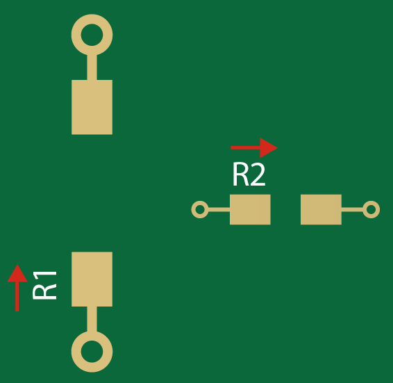
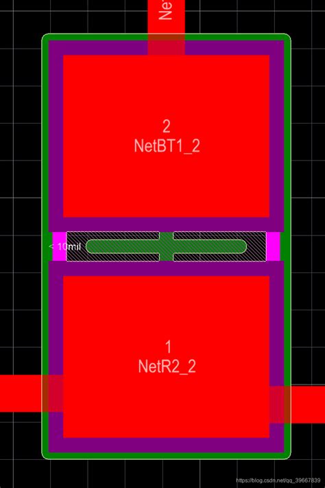
When designing advanced electronics, achieving microscopic accuracy in circuitry is non-negotiable. Additive PCB manufacturing eliminates the limitations of traditional etching by building conductive layers directly onto substrates, enabling traces as narrow as 15 microns. This precision ensures consistent signal integrity, even in high-frequency applications like 5G devices or IoT sensors. For PCB manufacturing companies, this translates to reduced material waste and fewer defects, directly lowering PCB manufacturing cost while maintaining tight tolerances.
By leveraging additive techniques, you gain the flexibility to create complex, multi-layered designs without compromising on reliability. Imagine embedding antennas or sensors directly into the board during production—a feat impractical with subtractive methods. Such capabilities are reshaping how PCB manufacturing businesses approach miniaturization and functionality, particularly in medical implants and aerospace systems.
Transitioning to additive processes also reduces dependency on hazardous chemicals, aligning with eco-conscious trends. As you adopt these methods, the balance between precision, efficiency, and sustainability becomes a competitive edge, ensuring your projects meet both technical and environmental benchmarks seamlessly.
Innovative Designs via Additive PCBs
Additive techniques are unlocking unprecedented design freedom in PCB manufacturing, allowing engineers to rethink traditional constraints. Unlike subtractive methods that carve away material, additive processes build circuits layer by layer, enabling intricate geometries, embedded components, and miniaturized layouts previously deemed unfeasible. This shift empowers PCB manufacturing companies to create high-density interconnects for wearables, IoT devices, and advanced medical equipment—all while reducing PCB manufacturing cost through material efficiency.
You’ll find that additive methods support rapid prototyping, letting design teams iterate complex layouts without costly tooling changes. For instance, 3D-printed conductive traces can integrate sensors directly into substrates, bypassing assembly steps that inflate production timelines. This agility is particularly valuable for startups in the PCB manufacturing business, where balancing innovation with budget constraints is critical.
Moreover, additive workflows enable hybrid designs combining rigid and flexible elements—ideal for foldable electronics or aerospace applications. By minimizing waste and supporting sustainable practices, these techniques align with evolving industry demands for eco-conscious production. As additive technologies mature, they’re not just reshaping how circuits are made but redefining what’s possible in electronic design altogether.
Eco-Friendly PCB Manufacturing Solutions
When evaluating PCB manufacturing processes, you might notice traditional methods often rely on subtractive techniques that generate excess waste. Additive approaches, however, prioritize sustainability by building circuits layer-by-layer, minimizing material usage and reducing chemical byproducts. For PCB manufacturing companies, this shift isn’t just about environmental responsibility—it’s a strategic move to lower PCB manufacturing cost while aligning with global eco-regulations.
By adopting additive methods, your PCB manufacturing business can cut raw material consumption by up to 70%, directly addressing concerns about resource efficiency. Unlike etching, which removes copper indiscriminately, additive processes deposit conductive traces precisely where needed, slashing hazardous waste. This precision also reduces energy demands, further shrinking your carbon footprint.
Eco-conscious consumers and industries increasingly favor partners who integrate sustainable practices. Additive techniques enable you to meet this demand without compromising on quality or design flexibility. As environmental regulations tighten globally, transitioning to greener methods positions your operations ahead of compliance curves while future-proofing your supply chain.
The ripple effect extends beyond cost savings: cleaner production cycles enhance brand reputation, attracting clients who prioritize sustainability. Whether you’re prototyping or scaling, additive methods offer a viable path to reconcile profitability with planetary stewardship—proving that innovation and ecology can coexist in modern electronics.
Future Trends in Additive Techniques
As additive techniques mature, you’ll see PCB manufacturing companies increasingly adopt multi-material printing to create circuits with embedded sensors or flexible substrates. Innovations like AI-driven design tools will refine precision further, enabling layouts that optimize signal integrity while reducing PCB manufacturing cost through material efficiency. Expect hybrid approaches combining additive and subtractive methods to dominate, balancing speed with micron-level accuracy for high-frequency applications.
Another key development is the shift toward closed-loop material systems, where waste from PCB manufacturing is recycled into new conductive inks. This aligns with global sustainability demands, making additive workflows indispensable for eco-conscious production. Meanwhile, advancements in nanoparticle-based inks will unlock higher conductivity at lower temperatures, opening doors for heat-sensitive components.
For the PCB manufacturing business, these trends mean faster time-to-market for prototypes and scalable solutions for complex designs. You’ll witness smaller enterprises leveraging desktop additive systems to compete with traditional factories, democratizing access to advanced circuitry. The future hinges on adaptability—those embracing these innovations will lead in delivering smarter, greener, and more cost-effective electronics.
Efficiency Gains in PCB Production
When evaluating PCB manufacturing processes, you’ll find that additive techniques significantly streamline production workflows. Unlike traditional subtractive methods—which involve etching away excess copper—additive approaches build circuits layer by layer, reducing material waste by up to 70%. This precision minimizes errors, allowing PCB manufacturing companies to accelerate prototyping cycles and deliver finished products faster.
By eliminating multiple steps like drilling and plating, additive methods cut PCB manufacturing cost while maintaining high-quality outputs. For example, direct printing of conductive inks reduces tooling expenses and energy consumption, making it ideal for low-to-medium volume orders. This efficiency is reshaping the PCB manufacturing business, enabling smaller firms to compete with larger players through agile, cost-effective production.
Transitioning to additive workflows also future-proofs operations. As demand grows for complex, miniaturized circuits, the ability to create intricate designs without additional labor or resources becomes a strategic advantage. This shift not only boosts productivity but aligns with broader industry trends toward sustainable, scalable solutions—ensuring your processes stay relevant in a rapidly evolving market.
Additive Methods Transforming Electronics
While traditional subtractive processes rely on etching away copper to create circuits, additive PCB manufacturing builds conductive pathways layer by layer. This approach allows PCB manufacturing companies to reduce material waste by up to 70%, directly addressing rising concerns about PCB manufacturing cost and environmental impact. By depositing conductive inks or pastes precisely where needed, you eliminate the need for chemical-heavy etching, making sustainable production a tangible reality.
The flexibility of additive techniques also unlocks unprecedented design freedom. Complex geometries, embedded components, and ultra-fine traces—once impractical with subtractive methods—are now achievable. For PCB manufacturing businesses, this means faster prototyping cycles and the ability to meet demands for miniaturized, high-performance devices. Imagine creating multilayer boards with 3D-printed interconnects or integrating sensors directly into substrates—innovations that redefine what’s possible in electronics.
This shift isn’t just about technical upgrades; it’s reshaping supply chains. With additive systems, you can localize production, cutting lead times and logistics expenses. As the industry pivots toward on-demand manufacturing, even small-scale PCB manufacturing ventures can compete globally. The result? A more agile, cost-effective ecosystem where innovation thrives without compromising efficiency or sustainability.
Conclusion
As PCB manufacturing evolves, additive techniques are fundamentally altering how you approach circuit board production. By minimizing material waste and energy consumption, these methods directly address rising concerns about PCB manufacturing cost while enhancing operational efficiency. For PCB manufacturing companies, adopting additive processes isn’t just about staying competitive—it’s about future-proofing your business in an industry increasingly driven by sustainability demands.
The precision of additive technology allows for unprecedented design flexibility, enabling your PCB manufacturing business to cater to cutting-edge applications without compromising on reliability. This shift not only reduces environmental impact but also opens doors to niche markets where traditional subtractive methods fall short. As material science advances, expect additive techniques to further streamline workflows, making low-volume, high-complexity projects more economically viable.
Ultimately, the transition to additive processes reflects a broader transformation in electronics—one where innovation and sustainability coexist. For forward-thinking manufacturers, integrating these methods today positions your operations at the forefront of tomorrow’s PCB manufacturing landscape.
Frequently Asked Questions
How does additive PCB manufacturing differ from traditional methods?
Additive techniques build circuits layer-by-layer using specialized materials, eliminating the need for etching. This reduces PCB manufacturing cost by minimizing material waste and energy use, while enabling complex designs that traditional methods struggle with.
Why should PCB manufacturing companies adopt additive processes?
Scalability and precision are key advantages. Additive methods allow PCB manufacturing companies to prototype faster, customize designs effortlessly, and maintain tighter tolerances—critical for high-frequency or miniaturized electronics.
Are additive PCBs reliable for high-volume production?
Yes. Modern additive systems achieve consistency comparable to subtractive methods, making them viable for both prototyping and mass production. This flexibility helps PCB manufacturing businesses optimize workflows and reduce time-to-market.
What environmental benefits do additive techniques offer?
By avoiding harsh chemicals and reducing copper waste, additive processes align with sustainable PCB manufacturing goals. Companies can lower their carbon footprint while meeting stricter environmental regulations.
How will additive technology shape future electronics?
Expect tighter integration with AI-driven design tools and broader material options, further lowering PCB manufacturing cost and unlocking innovations in wearables, IoT, and aerospace applications.
Ready to Explore Additive PCB Solutions?
For tailored guidance on integrating additive techniques into your production line, please click here to connect with industry experts at Andwin PCB.