Advanced assembly pcb-High quality & High precision
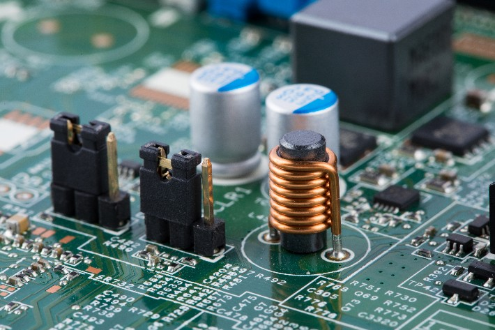
Advanced assembly PCB refers to the process of manufacturing printed circuit boards (PCBs) with complex designs and features.
This process involves the use of advanced technologies and techniques to produce high-quality PCBs that meet the specific requirements of the end-users.
Some of the features that are commonly found in advanced assembly PCBs include:
1. High-density interconnects (HDI):
These are circuits that have a high number of connections in a small area. HDI technology allows for the creation of smaller and more compact PCBs.
2. Microvias:
These are small holes that are drilled into the PCB to connect different layers of the circuit. Microvias allow for the creation of more complex and compact circuit designs.
3. Blind and buried vias:
These are vias that connect different layers of the PCB without going all the way through the board. Blind and buried vias allow for the creation of more complex and compact circuit designs.

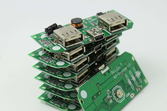
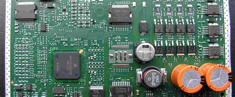
4. Surface mount technology (SMT):
This is a method of mounting components directly onto the surface of the PCB. SMT allows for the creation of smaller and more compact PCBs.
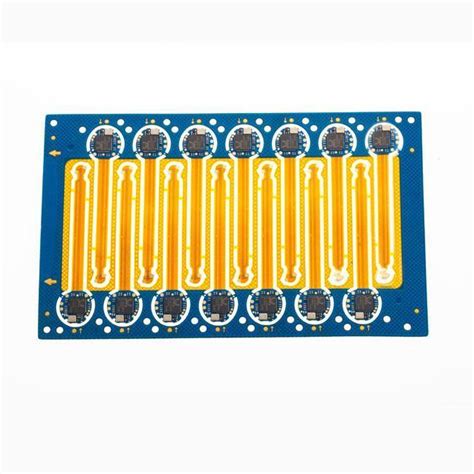
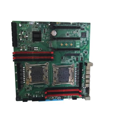
5. Multilayer PCBs:
These are PCBs that have multiple layers of circuits stacked on top of each other. Multilayer PCBs allow for the creation of more complex and compact circuit designs.
Advanced assembly PCBs are used in a wide range of applications, including aerospace, defense, medical, and telecommunications. These PCBs are typically manufactured using automated processes and require strict quality control measures to ensure their reliability and performance.

Quality control process of advance PCB assembly:
The quality control process of advance PCB assembly involves several steps to ensure that the final product meets the required standards and specifications. These steps include:
1. Inspection of raw materials:
The first step in the quality control process is to inspect the raw materials that will be used in the PCB assembly. This includes checking the quality of the PCBs, components, and other materials.
2. SMT assembly inspection:
After the surface mount technology (SMT) assembly process, the PCBs are inspected for any defects, such as missing components, incorrect placement, or soldering issues.
3. AOI inspection:
Automated optical inspection (AOI) is used to inspect the PCBs for any defects that may have been missed during the SMT assembly process. This includes checking for soldering defects, component placement, and other issues.

4. X-ray inspection:
X-ray inspection is used to check for any hidden defects, such as soldering issues or component placement.
5. Functional testing:
After the PCB assembly is complete, functional testing is conducted to ensure that the final product meets the required specifications and standards. This includes testing the PCBs for functionality, performance, and reliability.
6. Final inspection:
The final step in the quality control process is to conduct a final inspection of the PCB assembly to ensure that it meets all the required standards and specifications.
Overall, the quality control process of advance PCB assembly is critical to ensure that the final product is of high quality and meets the required standards and specifications.