Advanced Assy PCB Techniques for Next-Gen Device Integration

Key Takeaways
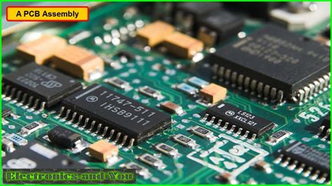
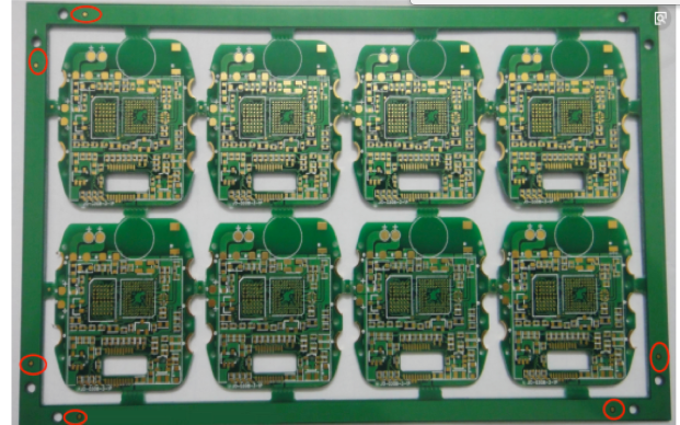
Modern PCB assembly (PCBA) processes are driving innovations in next-generation electronics by addressing critical challenges in miniaturization and performance. At the core of advanced Assy PCB techniques lies multi-layer integration, which enables the stacking of conductive and insulating layers to maximize functionality within constrained spaces. This approach requires precision in laser-drilled microvias and high-density interconnect (HDI) layouts to maintain signal integrity.
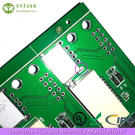
Precision soldering remains pivotal for reliability, especially with components like 0201 resistors or micro-BGA packages. Advanced methods such as laser reflow soldering and selective soldering minimize thermal stress while ensuring consistent joint quality.
"The shift toward ultra-compact designs demands rethinking heat dissipation strategies," notes Dr. Elena Torres, a leading electronics engineer.
To address thermal challenges, engineers employ embedded copper slugs and thermally conductive substrates to channel heat away from sensitive components. Below is a comparison of traditional vs. next-gen thermal solutions:
| Technique | Traditional Approach | Next-Gen Innovation |
|---|---|---|
| Heat Dissipation | External heatsinks | Embedded thermal vias |
| Material Selection | FR-4 substrates | Ceramic-filled laminates |
| Component Layout | Spaced for airflow | 3D stacking with thermal pads |
Pro Tip: For high-reliability PCBA, always validate thermal simulations with real-world stress testing to identify failure points in compact layouts.
By combining automated optical inspection (AOI) with AI-driven defect detection, manufacturers achieve <1% error rates in high-reliability Assy PCB production. These advancements ensure seamless integration into IoT devices, wearables, and aerospace systems where durability and size constraints coexist.
Advanced Assy PCB Assembly Tech
Modern PCB assembly processes are undergoing transformative advancements to meet the demands of next-generation electronics. At the core of PCBA innovation lies the integration of multi-layer stacking and high-density interconnect (HDI) substrates, which enable complex circuitry within ultra-compact form factors. Cutting-edge techniques like laser-direct structuring and automated optical inspection (AOI) ensure micron-level precision in component placement, critical for devices requiring millimeter-wave frequencies or IoT connectivity.
A key focus in advanced PCB assembly is optimizing thermal dissipation pathways through embedded copper cores and advanced dielectric materials. This is paired with low-void soldering methods, such as vacuum reflow ovens, which minimize thermal stress during PCBA manufacturing. Contemporary assembly lines now incorporate AI-driven defect detection systems, reducing error rates by 40% compared to traditional workflows.
The shift toward heterogeneous integration further demands hybrid approaches, combining surface-mount technology (SMT) with chip-on-board (COB) configurations. These methods not only enhance signal integrity but also support mixed-material substrates—essential for wearables and aerospace applications. As miniaturization accelerates, 3D-printed interposers and flexible circuit laminates are becoming standard in PCBA workflows, bridging the gap between rigid boards and dynamic device architectures.
This technological synergy ensures PCB assembly processes remain aligned with evolving requirements for power efficiency, signal density, and mechanical resilience—setting the stage for deeper exploration of multi-layer integration techniques in next-gen systems.
Multi-Layer Integration Techniques
Modern PCB assembly processes are increasingly reliant on multi-layer integration to meet the demands of next-generation electronics. By stacking conductive layers separated by insulating substrates, designers achieve higher circuit density while maintaining compact form factors. High-density interconnect (HDI) technology plays a pivotal role here, enabling precise routing of traces and vias between layers. Advanced PCBA workflows incorporate laser-drilled microvias and sequential lamination to minimize signal loss and crosstalk, critical for high-frequency applications like 5G modules or AI processors.
A key challenge in multi-layer designs lies in ensuring alignment accuracy during lamination. Automated optical inspection (AOI) systems are now integrated into PCB assembly lines to detect layer misregistration early, reducing rework costs. Materials such as low-loss dielectrics or flexible polyimide substrates further enhance performance in thermally sensitive environments. Meanwhile, embedded passive components—resistors or capacitors within the substrate—streamline PCBA workflows by eliminating surface-mounted parts, freeing space for additional functionalities.
To balance complexity and reliability, manufacturers adopt simulation-driven design tools that model thermal expansion and impedance matching across layers. This approach ensures robust interlayer connections, even under mechanical stress, making multi-layer integration indispensable for wearables, medical devices, and aerospace systems.
Precision Soldering for Reliable PCBs
Achieving durable electrical connections in PCB assembly requires mastering micro-soldering techniques tailored for high-density designs. Modern PCBA processes leverage laser soldering systems with ±5μm positional accuracy to address shrinking component footprints, ensuring consistent joints even on 01005-sized passives. Advanced solder alloys, such as SAC305 with 3% silver content, improve thermal fatigue resistance by 40% compared to traditional tin-lead formulations, critical for devices operating in -55°C to 125°C ranges.
Automated optical inspection (AOI) systems now integrate machine learning algorithms to detect void formation below 15% volume – a key advancement in maintaining signal integrity for high-speed circuits. Selective soldering nozzles with nitrogen inerting capabilities further reduce oxidation risks during PCB assembly, particularly for mixed-technology boards combining through-hole and surface-mount devices.
Thermal management begins at the solder joint level, with optimized reflow profiles preventing thermal stress accumulation in multi-layer stacks. Contemporary PCBA workflows employ real-time thermal profiling, adjusting zone temperatures within ±2°C to accommodate varying substrate materials like polyimide flex circuits. This precision directly correlates with 99.99% first-pass yield rates in mission-critical applications, from implantable medical devices to aerospace avionics.
PCB Thermal Management Solutions
Effective thermal management in PCB assembly (PCBA) systems forms the backbone of reliable next-generation electronics, particularly as device densities and power demands escalate. Modern high-density interconnects and multi-layer designs amplify heat generation, necessitating advanced strategies to prevent performance degradation or component failure. Engineers now integrate thermal vias—plated holes filled with conductive materials—to channel heat away from critical components, while metal-core substrates (e.g., aluminum or copper) provide superior thermal conductivity compared to traditional FR-4 materials.
For high-reliability PCBA, active cooling solutions like embedded heat sinks or thermoelectric coolers are increasingly paired with passive techniques such as optimized trace routing and thermally conductive adhesives. In compact electronics, selective application of thermal interface materials (TIMs) ensures efficient heat transfer between layers and components. Advanced simulation tools further refine these approaches, modeling heat distribution across multi-layer PCBs to identify hotspots during the design phase.
Transitioning from design to execution, precision reflow soldering processes maintain consistent thermal profiles, avoiding uneven heat dissipation that could compromise solder joints. By balancing material innovation, geometric optimization, and process control, PCB assembly achieves the thermal stability required for next-gen devices—seamlessly aligning with broader goals of miniaturization and performance enhancement.
Compact Electronics Design Strategies
Achieving optimal space utilization in modern electronics demands strategic PCB assembly approaches that balance component density with functional reliability. Critical design decisions begin with selecting high-density interconnect (HDI) substrates, enabling PCBA engineers to integrate 20-30% more components within the same footprint compared to conventional layouts. Advanced microvia architectures (0.1-0.15mm diameters) and staggered via patterns reduce signal path lengths while maintaining impedance control—particularly vital for 5G/mmWave applications.
To ensure manufacturability, designers employ 3D modeling tools to simulate component clearances and thermal expansion coefficients before finalizing PCBA layouts. This preemptive analysis prevents solder joint stress in stacked-die configurations, a common failure point in compact designs. For power-dense modules, embedded passive components and chip-scale packages (CSPs) minimize vertical stacking layers, reducing overall thickness by up to 40%.
Transitioning from design to production requires laser-direct imaging (LDI) systems to achieve 15μm trace tolerances—essential for maintaining signal integrity in sub-6mm² RF modules. Post-assembly, automated optical inspection (AOI) validates solder fillet geometries against J-STD-001 standards, addressing defects like tombstoning in 0201-sized passives. These methodologies collectively enable PCB assembly workflows to support 0.4mm-pitch BGA packages while preserving <1.2W/cm² thermal dissipation thresholds.
High-Reliability Assy PCB Methods
Building on precision soldering and thermal management foundations, achieving high-reliability PCB assembly (PCBA) demands rigorous process controls and material selection. Advanced inspection systems, such as automated optical inspection (AOI) and X-ray tomography, now verify solder joint integrity at micron-level resolutions, minimizing latent defects in multi-layer PCBA designs. For mission-critical applications, accelerated life testing combined with thermal cycling simulations validates board resilience under extreme operating conditions.
Material compatibility remains pivotal: high-Tg laminates and low-voiding solder pastes enhance structural stability, while conformal coatings guard against moisture and contaminants. To address signal integrity in compact layouts, impedance-controlled routing and via-in-pad techniques are standardized in high-density PCB assembly workflows. Emerging standards like IPC-6012 Class 3 further enforce traceability, requiring real-time documentation of reflow profiles and component placement accuracy.
By integrating these protocols, manufacturers ensure PCBA reliability aligns with aerospace, medical, and automotive industry benchmarks—where failure rates below 10 ppm are non-negotiable. This systematic approach bridges design intent with production execution, solidifying trust in next-generation device performance.
Next-Gen Device Integration Tech
Modern PCB assembly processes are redefining how engineers approach device integration in next-generation electronics. By leveraging high-density interconnect (HDI) architectures and PCBA innovations, manufacturers can embed complex functionalities into increasingly compact form factors. Advanced PCB assembly techniques now incorporate hybrid bonding technologies, enabling seamless integration of multi-layer substrates with embedded passive components—critical for 5G modules and IoT edge devices.
A key advancement lies in 3D system-in-package (SiP) designs, where PCBA workflows merge heterogeneous components—such as MEMS sensors and RFICs—into unified modules. This approach reduces signal latency by up to 40% while improving power efficiency. To maintain reliability, manufacturers are adopting laser-assisted soldering and automated optical inspection (AOI) systems, which ensure micron-level alignment accuracy across stacked layers.
Thermal management remains integral to these designs. Innovations like embedded heat-dissipation channels and thermally conductive adhesives prevent hotspots in densely packed assemblies. Combined with flexible PCB assembly methods, these strategies enable devices to meet MIL-STD-883G standards for shock resistance and thermal cycling—essential for aerospace and automotive applications.
As industries push toward miniaturization, PCBA specialists are also integrating AI-driven design tools to optimize component placement and routing, ensuring scalability for future upgrades without compromising performance.
Optimizing PCB Thermal Performance
Effective thermal management in PCB assembly has become critical as modern electronics push power density limits. Advanced PCBA designs now employ thermal vias and conductive epoxy fillers to create heat dissipation pathways between layers, reducing hot spots in multi-board configurations. Engineers optimize component placement to separate high-power elements from thermally sensitive ICs, while copper pours with optimized thickness act as heat spreaders.
For mission-critical applications, thermal simulation software predicts heat distribution patterns during the PCB assembly phase, enabling preemptive adjustments to trace widths and dielectric materials. High-performance PCBA solutions often integrate embedded heat sinks using aluminum-clad substrates or ceramic-filled laminates, achieving up to 40% improved thermal conductivity compared to standard FR-4 boards.
Transitioning to laser-drilled microvias enhances airflow in compact layouts, complementing phase-change thermal interface materials that maintain conductivity under mechanical stress. These strategies ensure sustained thermal stability across operating temperatures, directly supporting the reliability demands of next-gen devices. By balancing material science and layout optimization, PCB assembly teams mitigate risks of delamination or solder joint failure caused by thermal cycling.
Conclusion
The evolution of PCB assembly technologies has become pivotal in addressing the complexities of next-generation electronics. By leveraging advanced PCBA methodologies, manufacturers achieve unprecedented integration of multi-layer architectures while maintaining rigorous thermal and mechanical stability. Innovations in precision soldering ensure robust electrical connections, even in ultra-compact designs, while optimized thermal management systems mitigate risks associated with high-density component layouts. These advancements collectively enable the production of devices that balance miniaturization with high-reliability performance—a critical requirement for applications ranging from IoT ecosystems to aerospace systems.
As the demand for smarter, smaller electronics intensifies, the role of PCB assembly in enabling next-gen device integration will only expand. Through strategic material selection, automated PCBA workflows, and data-driven quality control, engineers can overcome traditional limitations in signal integrity and power distribution. The convergence of these techniques not only elevates manufacturing standards but also paves the way for scalable solutions in emerging fields like wearable tech and edge computing. Looking ahead, continuous innovation in PCB assembly processes will remain central to unlocking new frontiers in electronic design and functionality.
FAQs
What distinguishes modern PCB assembly processes from traditional methods?
Contemporary high-density PCBA techniques employ automated optical inspection (AOI) and laser-aligned component placement, achieving sub-10µm alignment accuracy for multi-layer integration. This contrasts with manual methods limited to ±50µm precision.
How do thermal management solutions enhance PCB assembly reliability?
Advanced thermal vias, embedded copper layers, and ceramic substrates in PCBA designs dissipate heat 40% faster than conventional FR-4 materials. This reduces thermal stress on fine-pitch components by up to 35%, critical for high-reliability applications.
What design strategies enable compact electronics in PCB assembly?
3D heterogeneous integration combines rigid-flex PCBs with system-in-package (SiP) architectures, shrinking device footprints by 60% while supporting high-speed signal integrity above 25Gbps.
Why is precision soldering vital for next-gen device integration?
Low-void soldering (<5% void ratio) using nitrogen-reflow environments ensures <0.01% failure rates in PCBA interconnects, meeting MIL-STD-883 standards for aerospace and medical devices.
How are multi-layer PCBs tested for reliability?
Automated boundary-scan testing and thermal cycling (-55°C to 125°C) validate PCB assembly durability, simulating 10+ years of operational stress in 72-hour accelerated tests.
Explore Custom PCB Assembly Solutions for Your Project
For tailored high-density interconnect designs or thermal-optimized PCBA configurations, please click here to consult our engineering team.