Advanced circuits pcb assembly
Innovations In Advanced Circuit PCB Assembly Techniques
In recent years, the field of advanced circuit PCB (Printed Circuit Board) assembly has witnessed significant innovations, driven by the increasing demand for more efficient, compact, and reliable electronic devices.
As technology continues to evolve, the need for sophisticated PCB assembly techniques has become paramount, enabling manufacturers to meet the stringent requirements of modern electronic applications. This article explores some of the key innovations in advanced circuit PCB assembly techniques, highlighting their impact on the electronics industry.
One of the most notable advancements in PCB assembly is the development of surface mount technology (SMT).
SMT has revolutionized the way electronic components are mounted onto PCBs, allowing for smaller and more densely packed boards. By enabling components to be mounted directly onto the surface of the board, SMT eliminates the need for drilling holes, which was a requirement in traditional through-hole technology.
This not only reduces manufacturing time and costs but also enhances the performance and reliability of the final product.
Moreover, SMT facilitates the integration of more complex circuits, which is essential for modern electronic devices that demand high functionality in compact forms.
In addition to SMT, the advent of advanced materials has played a crucial role in enhancing PCB assembly techniques.
The use of high-performance substrates, such as polyimide and ceramic, has improved the thermal and electrical properties of PCBs, making them suitable for high-frequency and high-power applications.
These materials offer superior heat dissipation and electrical insulation, which are critical for maintaining the integrity and longevity of electronic components.
Furthermore, the incorporation of advanced materials has enabled the development of flexible PCBs, which are increasingly used in applications where space constraints and mechanical flexibility are key considerations.
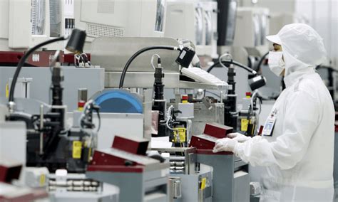
Another significant innovation in PCB assembly is the implementation of automated assembly processes.
Automation has transformed the manufacturing landscape by increasing precision, reducing human error, and enhancing production efficiency. Automated pick-and-place machines, for instance, can accurately position components on a PCB at high speeds, ensuring consistent quality and reducing the likelihood of defects.
Additionally, automated optical inspection (AOI) systems have become integral to the assembly process, providing real-time quality control by detecting defects and ensuring that each board meets the required specifications.
The integration of advanced testing and inspection techniques has further bolstered the reliability of PCB assemblies.
Techniques such as in-circuit testing (ICT) and functional testing are employed to verify the performance and functionality of assembled boards. These testing methods help identify potential issues early in the production process, allowing for timely corrective actions and minimizing the risk of faulty products reaching the market. Moreover, the use of X-ray inspection technology has become increasingly prevalent, enabling manufacturers to examine the internal structure of PCBs and detect hidden defects that are not visible to the naked eye.
As the demand for more sophisticated electronic devices continues to grow, the importance of advanced circuit PCB assembly techniques cannot be overstated.
The innovations discussed in this article represent just a fraction of the ongoing advancements in this field. As technology progresses, it is expected that further developments will continue to enhance the capabilities of PCB assembly, paving the way for even more complex and efficient electronic devices.
Ultimately, these innovations not only benefit manufacturers by improving production processes but also contribute to the advancement of technology as a whole, enabling the creation of cutting-edge products that meet the ever-evolving needs of consumers.
Challenges And Solutions In High-Density PCB Assembly
In the realm of advanced circuits, high-density printed circuit board (PCB) assembly presents a unique set of challenges that demand innovative solutions.
As electronic devices continue to shrink in size while increasing in functionality, the need for compact and efficient PCB designs has become paramount.
This trend towards miniaturization necessitates the integration of more components into smaller spaces, thereby increasing the complexity of PCB assembly processes. Consequently, manufacturers face several challenges, including component placement accuracy, thermal management, and signal integrity, each of which requires careful consideration and strategic solutions.
One of the primary challenges in high-density PCB assembly is the precise placement of components.
As the size of components decreases and the number of connections increases, the margin for error becomes significantly smaller. To address this, manufacturers employ advanced pick-and-place machines equipped with high-resolution cameras and sophisticated algorithms. These machines are capable of placing components with remarkable accuracy, ensuring that each part is correctly aligned and positioned.
Additionally, the use of automated optical inspection (AOI) systems further enhances accuracy by detecting misalignments and defects early in the assembly process, thereby reducing the likelihood of costly rework.
Another significant challenge is thermal management. As more components are packed into a smaller area, the heat generated during operation can lead to overheating, which may compromise the performance and reliability of the PCB.
To mitigate this issue, designers incorporate thermal vias, heat sinks, and advanced materials with high thermal conductivity into the PCB design. These solutions facilitate efficient heat dissipation, maintaining optimal operating temperatures and ensuring the longevity of the electronic device.
Moreover, the use of thermal simulation software during the design phase allows engineers to predict and address potential thermal issues before the manufacturing process begins.
Signal integrity is also a critical concern in high-density PCB assembly.
As the density of interconnections increases, so does the potential for signal interference and crosstalk, which can degrade the performance of the circuit. To combat this, designers employ techniques such as controlled impedance routing, differential signaling, and the use of ground planes to minimize electromagnetic interference. Additionally, advanced simulation tools enable engineers to model and analyze signal behavior, allowing them to optimize the layout for maximum signal integrity.
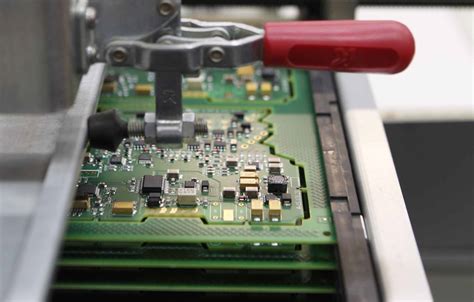
Furthermore, the advent of surface mount technology (SMT) has revolutionized high-density PCB assembly by allowing components to be mounted directly onto the surface of the board, rather than through-hole mounting.
This technology not only saves space but also enhances the reliability and performance of the circuit. However, SMT requires precise soldering techniques to ensure strong and reliable connections. To achieve this, manufacturers utilize reflow soldering processes, which involve carefully controlled heating profiles to melt solder paste and form secure bonds between components and the PCB.
In conclusion, while high-density PCB assembly presents a myriad of challenges, the industry has developed a range of solutions to address these issues effectively.
Through the use of advanced machinery, innovative design techniques, and cutting-edge simulation tools, manufacturers can overcome the obstacles associated with component placement, thermal management, and signal integrity. As technology continues to evolve, the ongoing development of new materials and methods will undoubtedly further enhance the capabilities of high-density PCB assembly, paving the way for even more compact and powerful electronic devices.
The Role Of Automation In Advanced PCB Assembly
In the rapidly evolving landscape of electronics manufacturing, the role of automation in advanced printed circuit board (PCB) assembly has become increasingly pivotal. As the demand for more complex and miniaturized electronic devices grows, manufacturers are compelled to adopt innovative solutions to enhance efficiency, precision, and reliability in PCB assembly processes. Automation, therefore, emerges as a critical component in meeting these demands, offering numerous advantages that traditional manual assembly methods cannot match.
To begin with, automation significantly enhances the precision and accuracy of PCB assembly.
Automated systems are equipped with advanced technologies such as robotic arms, machine vision, and sophisticated software algorithms that ensure components are placed with exacting precision. This level of accuracy is particularly crucial in advanced circuits where even the slightest misalignment can lead to functional failures or reduced performance. By minimizing human error, automation ensures that each PCB meets stringent quality standards, thereby reducing the likelihood of defects and the need for costly rework.
Moreover, automation in PCB assembly contributes to increased production speed and efficiency.
Automated assembly lines can operate continuously, without the fatigue or inconsistency associated with human labor. This capability allows manufacturers to scale up production to meet high-volume demands without compromising on quality. Additionally, automated systems can quickly adapt to design changes or new product introductions, providing manufacturers with the flexibility needed to stay competitive in a fast-paced market. This adaptability is particularly beneficial in industries such as consumer electronics and telecommunications, where product lifecycles are short and innovation is constant.
In addition to speed and precision, automation also plays a crucial role in enhancing the reliability and consistency of PCB assembly processes.
Automated systems are designed to perform repetitive tasks with unwavering consistency, ensuring that each PCB produced is identical to the last. This uniformity is essential for maintaining product reliability, especially in applications where PCBs are subjected to harsh environments or critical operations, such as in aerospace or medical devices. By ensuring consistent quality, automation helps manufacturers build trust with their customers and maintain a strong reputation in the market.
Furthermore, automation in PCB assembly can lead to significant cost savings over time.
While the initial investment in automated equipment may be substantial, the long-term benefits often outweigh these costs. Automation reduces the need for manual labor, lowers the incidence of defects, and minimizes material waste, all of which contribute to a more cost-effective production process. Additionally, the ability to produce high-quality PCBs at a faster rate can lead to increased revenue opportunities, further justifying the investment in automation.
Despite these advantages, it is important to acknowledge that the integration of automation in PCB assembly is not without its challenges.
Manufacturers must carefully consider factors such as equipment compatibility, process optimization, and workforce training to fully realize the benefits of automation. However, with careful planning and execution, these challenges can be effectively managed, paving the way for a more efficient and advanced PCB assembly process.
In conclusion, the role of automation in advanced PCB assembly is undeniably transformative. By enhancing precision, speed, reliability, and cost-effectiveness, automation enables manufacturers to meet the growing demands of the electronics industry while maintaining high standards of quality. As technology continues to advance, the integration of automation in PCB assembly will likely become even more sophisticated, further solidifying its role as a cornerstone of modern electronics manufacturing.
Quality Control Measures In Advanced Circuit PCB Assembly
In the realm of advanced circuit PCB assembly, quality control measures are paramount to ensuring the reliability and functionality of electronic devices. As technology continues to evolve, the complexity of printed circuit boards (PCBs) has increased, necessitating rigorous quality control protocols to maintain high standards. These measures are integral to the assembly process, as they help identify and rectify potential defects that could compromise the performance of the final product.
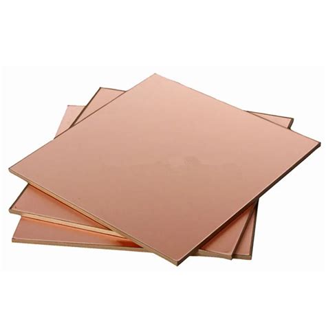
To begin with, the foundation of quality control in PCB assembly lies in the meticulous inspection of raw materials.
Ensuring that components such as substrates, copper foils, and solder masks meet specified standards is crucial. This initial step prevents defects from propagating through subsequent stages of assembly. Furthermore, suppliers are often required to provide certification of compliance with industry standards, which serves as an additional layer of assurance.
As the assembly process progresses, automated optical inspection (AOI) systems play a pivotal role in maintaining quality.
These systems utilize high-resolution cameras to capture images of the PCB and compare them against a predefined set of criteria. By identifying discrepancies such as misaligned components or soldering defects, AOI systems enable swift corrective actions, thereby minimizing the risk of faulty assemblies reaching the next stage.
In addition to AOI, X-ray inspection is employed to examine the integrity of solder joints, particularly in cases where components are densely packed or obscured by other elements.
This non-destructive testing method provides a detailed view of the internal structure of solder joints, allowing for the detection of voids, cracks, or insufficient solder coverage. By addressing these issues early in the assembly process, manufacturers can prevent potential failures in the field.
Moreover, functional testing is a critical component of quality control in advanced circuit PCB assembly.
This involves subjecting the assembled PCB to a series of tests that simulate real-world operating conditions. By verifying that the board performs as intended, functional testing ensures that any latent defects are identified before the product is shipped to customers. This step is particularly important for high-reliability applications, such as aerospace or medical devices, where failure is not an option.
Transitioning from testing to process control, statistical process control (SPC) techniques are employed to monitor and control the assembly process.
By analyzing data collected during production, manufacturers can identify trends and variations that may indicate potential quality issues. Implementing SPC allows for continuous improvement, as it provides insights into process stability and capability, enabling manufacturers to make informed decisions about process adjustments.
Furthermore, the importance of traceability in quality control cannot be overstated.
By maintaining detailed records of each component and process step, manufacturers can quickly identify the root cause of any defects that arise. This traceability is essential for effective problem-solving and ensures that corrective actions are both timely and targeted.
In conclusion, quality control measures in advanced circuit PCB assembly are multifaceted and encompass a range of techniques and technologies. From the inspection of raw materials to the implementation of sophisticated testing and process control methods, each step is designed to ensure the highest level of quality and reliability. As the demand for complex electronic devices continues to grow, the importance of these measures will only increase, underscoring their critical role in the success of PCB assembly operations.


