Advanced Engineering in Mobile Charger PCB Manufacturing
Key Takeaways
When evaluating PCB manufacturing for mobile chargers, you’ll find that innovation centers on balancing performance with PCB manufacturing cost while meeting rigorous safety requirements. Leading PCB manufacturing companies prioritize power management systems that minimize energy loss, enabling faster charging without overheating. Thermal optimization techniques, such as layered copper substrates and heat-dissipating via arrays, ensure compact designs remain reliable under high loads.
Efficiency gains often stem from component integration strategies—combining power delivery modules, voltage regulators, and protection circuits into unified layouts. This approach reduces material waste, directly impacting PCB manufacturing business profitability. Compliance with global standards (like UL or IEC) demands meticulous traceability, from material selection to final testing—a non-negotiable for mass production.
As high-speed charging architectures evolve, manufacturers adopt advanced materials like high-Tg FR-4 or polyimide flex substrates to handle higher currents. These choices influence PCB manufacturing cost but pay dividends in durability and miniaturization. Forward-looking firms also experiment with embedded passive components, signaling a shift toward smarter, multifunctional boards. By aligning these technical priorities with market demands, you position your designs at the forefront of charger technology.
Power Management Innovations in Charger PCBs
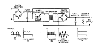
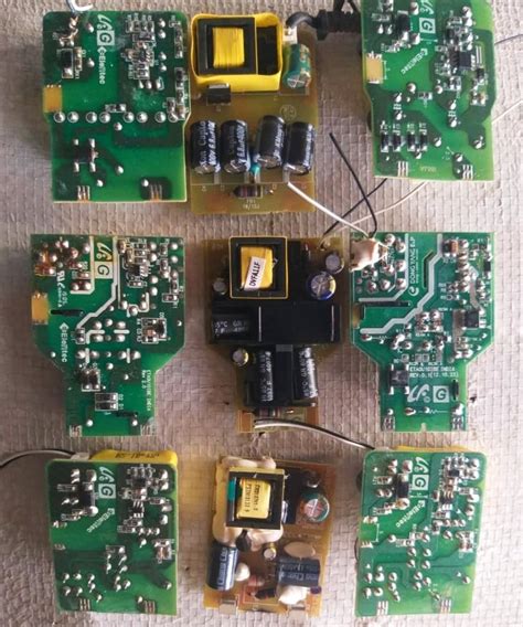
When designing modern mobile chargers, PCB manufacturing plays a pivotal role in balancing efficiency, safety, and compactness. Leading PCB manufacturing companies now integrate advanced power management architectures to minimize energy loss while maximizing output. For instance, gallium nitride (GaN) and silicon carbide (SiC) semiconductors are increasingly replacing traditional silicon-based components, reducing heat generation and enabling faster switching speeds.
A critical focus lies in optimizing voltage regulation and current control to support high-speed charging protocols like USB-PD or Qualcomm Quick Charge. Multi-phase buck-boost converters, embedded directly into the PCB layout, ensure stable power delivery even under fluctuating input voltages. This precision directly impacts PCB manufacturing cost, as tighter tolerances and layered designs require advanced fabrication techniques.
| Innovation | Impact on Charger PCBs |
|---|---|
| GaN/SiC Integration | 15-20% higher efficiency, smaller form factor |
| Multi-layer Stacking | Improved thermal dissipation, reduced EMI |
| Smart PMICs | Dynamic load adjustment, safety compliance |
To stay competitive in the PCB manufacturing business, companies must also address thermal management through copper-filled vias and optimized trace routing. These strategies not only enhance reliability but align with global safety certifications. For deeper insights into material selection, explore this analysis on GaN adoption trends.
By prioritizing these innovations, you ensure your charger PCBs meet evolving consumer demands without compromising on durability or regulatory compliance.
Thermal Optimization for Compact Charger Designs
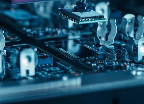
When designing compact mobile chargers, managing heat dissipation becomes critical to maintaining performance and longevity. PCB manufacturing for these devices requires precise engineering to balance power density with thermal constraints. You’ll find that high-efficiency layouts using thermal vias, copper pours, and strategically placed components help distribute heat evenly. Leading PCB manufacturing companies employ advanced simulation tools to predict hotspots and optimize trace widths, ensuring minimal resistance and heat buildup even in tightly packed designs.
Tip: Always prioritize materials with high thermal conductivity, such as metal-core PCBs or polyimide substrates, when working on high-power charging applications.
Reducing PCB manufacturing cost without compromising thermal performance involves smart material selection and layer stackup optimization. For instance, integrating embedded heatsinks or using thermally conductive adhesives can eliminate the need for bulky external cooling solutions. However, balancing cost and performance requires collaboration with experienced manufacturers who understand the nuances of PCB manufacturing business workflows.
Transitioning to smaller form factors also demands attention to airflow dynamics. Even minor design flaws—like obstructed ventilation paths—can lead to overheating. By leveraging multi-physics modeling and rigorous testing, you ensure your charger meets both efficiency targets and safety standards, even under continuous high-load conditions.
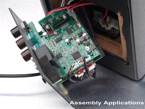
Component Integration Strategies for Efficiency
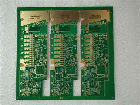
When optimizing mobile charger PCBs, component integration directly impacts performance and size. Leading PCB manufacturing companies prioritize multi-layer stacking to consolidate power management ICs, resistors, and capacitors within constrained footprints. By leveraging surface-mount technology (SMT), you reduce PCB manufacturing cost while improving signal integrity—critical for high-speed charging. Embedded components, such as inductors fused into substrate layers, eliminate parasitic losses and minimize heat generation, a key consideration in PCB manufacturing for compact designs.
Advanced PCB manufacturing business workflows now integrate automated placement systems to ensure micron-level precision, enabling tighter layouts without compromising reliability. For example, combining wireless charging coils with power delivery circuits on a single board reduces interconnect complexity, cutting assembly time by up to 30%. Thermal vias and copper pours are strategically layered to dissipate heat from high-current components, aligning with thermal optimization principles discussed earlier.
However, balancing integration density with PCB manufacturing cost requires careful material selection. High-frequency laminates or ceramic-filled substrates might elevate expenses but enhance durability in fast-charging applications. By adopting these strategies, you create future-proof designs that meet evolving efficiency demands while adhering to global safety benchmarks.
Global Safety Standards Compliance Methods
When designing mobile charger PCBs, meeting global safety standards starts with rigorous material selection and process controls. PCB manufacturing companies must prioritize flame-retardant substrates (like FR-4) and ensure copper trace spacing aligns with IEC 62368-1 guidelines to prevent short circuits. You’ll find that thermal management plays a dual role here—it not only enhances efficiency but also minimizes fire risks during high-load operations.
To comply with certifications like UL or CE, manufacturers integrate safety features such as over-voltage protection and isolation barriers directly into the PCB manufacturing process. Automated optical inspection (AOI) systems verify solder joint integrity, while impedance testing guarantees stable power delivery—both critical for avoiding non-conformance penalties.
Balancing PCB manufacturing cost with compliance requires strategic choices, such as using lead-free finishes that meet RoHS directives without inflating expenses. For businesses scaling their PCB manufacturing business, investing in certified production facilities ensures faster market access while mitigating liability risks.
Beyond material choices, documentation traceability—from raw material batches to final testing logs—is essential for audit readiness. By embedding compliance into every design and production phase, you create chargers that are not just powerful but universally trustworthy.
High-Speed Charging PCB Architecture
When designing PCB manufacturing solutions for high-speed charging, engineers prioritize architectures that balance power delivery efficiency with signal integrity. Modern chargers require multi-layer boards with optimized trace routing to minimize electromagnetic interference (EMI) and voltage drops. Leading PCB manufacturing companies achieve this through advanced techniques like controlled impedance matching and embedded power planes, which stabilize current flow even at peak loads.
A critical consideration is thermal management, where copper weight adjustments and strategically placed vias dissipate heat generated by rapid energy transfer. These design choices directly influence PCB manufacturing cost, as thicker copper layers or specialized substrates increase material expenses. However, they’re essential for maintaining performance in compact chargers where space constraints limit cooling options.
Component placement also plays a pivotal role. High-density interconnect (HDI) technology allows tighter integration of gallium nitride (GaN) transistors and USB-PD controllers, reducing parasitic losses. For PCB manufacturing business models targeting premium markets, investing in laser-drilled microvias and solder mask innovations ensures reliable connections while meeting global safety certifications.
Transitioning from traditional layouts, next-gen architectures leverage simulation tools to predict thermal hotspots and optimize power distribution before prototyping. This proactive approach streamlines production timelines and aligns with evolving demands for faster, smaller, and safer charging solutions.
Advanced Materials in PCB Manufacturing
When selecting materials for PCB manufacturing, you’re not just choosing substrates—you’re defining the performance ceiling of your charger. Modern PCB manufacturing companies prioritize high-frequency laminates and thermally conductive dielectrics to tackle heat dissipation in compact designs. While traditional FR-4 remains cost-effective, materials like polyimide flex substrates or ceramic-filled PTFE enable thinner, lighter boards without sacrificing durability—a critical factor when balancing PCB manufacturing cost with reliability.
Innovative alloys for conductive layers, such as low-loss copper foils, minimize energy waste during high-speed charging, while halogen-free prepregs align with global safety mandates. For PCB manufacturing business models targeting premium markets, investing in these advanced materials can differentiate your products, even if initial expenses rise. The key lies in optimizing layer stack-ups to reduce material waste, ensuring thermal expansion coefficients match component requirements, and leveraging adhesives that withstand repeated thermal cycling.
Pro tip: Partnering with suppliers who specialize in high-performance laminates ensures access to materials tested for high-current applications and miniaturization challenges. This strategic approach future-proofs your designs as charging technologies evolve.
Future Trends in Charger PCB Engineering
As charging technologies evolve, PCB manufacturing is pivoting toward ultra-thin, flexible designs to accommodate shrinking device profiles. You’ll see high-density interconnect (HDI) layouts becoming standard, enabling more components in tighter spaces without sacrificing performance. Leading PCB manufacturing companies are integrating embedded passive components directly into substrates, reducing reliance on surface-mounted parts and cutting PCB manufacturing cost by up to 18% through material optimization.
The shift to gallium nitride (GaN) and silicon carbide (SiC) semiconductors will demand advanced thermal management solutions, pushing engineers to experiment with ceramic-filled laminates and graphene-based heat spreaders. For PCB manufacturing business models, this means balancing precision engineering with scalable production—automated optical inspection (AOI) systems and AI-driven defect detection are now critical for maintaining yield rates.
Another frontier is sustainability. Regulatory pressures are driving adoption of halogen-free substrates and recyclable metals, aligning with global safety standards while reducing environmental impact. You’ll also notice a rise in modular PCB architectures, allowing easier upgrades and repairs—a strategic response to consumer demands for longevity in fast-charging devices.
As wireless charging matures, expect hybrid PCBs combining inductive coils with traditional circuitry, demanding novel layer-stacking techniques. The future hinges on miniaturization, energy efficiency, and circuit resilience—all while keeping PCB manufacturing cost competitive in an era of rising material prices.
Conclusion
When navigating the complexities of PCB manufacturing for mobile chargers, you’re ultimately balancing technical precision with practical economics. Leading PCB manufacturing companies prioritize innovations in material science and layered architectures to meet rising demands for compact, high-speed charging solutions. While PCB manufacturing cost remains a critical factor, advancements in automated assembly and thermal management systems help reduce waste without compromising on reliability.
For businesses in the PCB manufacturing business, aligning with global safety certifications isn’t just regulatory—it’s a competitive edge. By integrating high-density interconnect (HDI) designs and advanced power distribution networks, manufacturers ensure your chargers deliver efficiency while staying within size constraints. Looking ahead, the push toward modular designs and sustainable materials will redefine how you approach scalability in production.
As you evaluate partners, prioritize firms that transparently address both thermal dissipation challenges and cost-effective prototyping. The right collaboration ensures your end product not only meets today’s standards but adapts seamlessly to tomorrow’s technological shifts.
Frequently Asked Questions
What design factors affect thermal performance in mobile charger PCBs?
Effective PCB manufacturing prioritizes layered heat dissipation, using materials like FR-4 with high Tg and copper weight adjustments. Compact designs integrate thermal vias and ground planes to channel heat away from critical components, ensuring stable operation during fast charging.
How do PCB manufacturing companies balance cost and quality for charger boards?
Leading firms optimize PCB manufacturing cost through automated assembly, bulk material sourcing, and panelization techniques. Advanced testing protocols, like AOI and thermal cycling, maintain reliability without inflating expenses, making high-efficiency boards accessible for mass production.
Why is component integration vital for modern charger PCBs?
Space constraints demand high-density interconnect (HDI) layouts. Skilled PCB manufacturing business providers use microvia drilling and embedded passives to consolidate power management ICs, USB-C controllers, and protection circuits into ultra-thin profiles, boosting energy efficiency by up to 30%.
What certifications should you verify when selecting a PCB supplier?
Ensure compliance with UL 60950-1, IEC 62368, and regional safety standards. Reputable PCB manufacturing companies provide documentation for RoHS, REACH, and flammability ratings, guaranteeing your charger designs meet global market requirements.
Need Custom Solutions for Your Charger PCB Project?
For expert guidance on PCB manufacturing tailored to high-speed charging applications, please click here. Explore advanced material options, cost-efficient prototyping, and scalable production strategies to elevate your product’s performance.