Advanced Flex Board Fabrication: Design Principles and Material Optimization

Key Takeaways
When optimizing flex PCB manufacturing, understanding bend radius calculations becomes critical to prevent conductor fatigue. You’ll need to balance PCB manufacturing cost with durability by selecting materials like polyimide or liquid crystal polymer, which excel in dynamic flexing applications. For space-saving layouts, prioritize staggered traces and avoid 90-degree angles to minimize stress points—a strategy often refined by leading PCB manufacturing companies.
Tip: Always validate your bend radius against the material’s elongation properties during prototyping to avoid premature failure in high-flex environments.
Lightweight designs benefit from thinner copper layers and adhesiveless constructions, which reduce bulk without compromising performance. When designing for harsh environments, consider hybrid flex-rigid transition zones to enhance mechanical stability while maintaining signal integrity. Partnering with PCB manufacturing businesses that specialize in advanced materials ensures your designs meet thermal and chemical resistance requirements. For deeper insights into material trade-offs, explore this resource on flex circuit optimization.
By integrating these principles, you’ll create circuits that endure repetitive bending, reduce assembly complexity, and align with cost-efficient PCB manufacturing workflows—key factors for next-generation electronics.

Flex PCB Bend Radius Optimization
When designing flexible circuits, calculating the optimal bend radius is critical to ensure reliability without compromising performance. A smaller radius may save space, but exceeding material limits risks microcracking or delamination. For PCB manufacturing teams, balancing mechanical stress and electrical integrity starts with understanding your application’s flex cycle requirements—whether it’s a one-time installation or dynamic bending.
Material properties directly influence bend tolerance. Polyimide substrates, common in PCB manufacturing companies, typically handle tighter radii than thicker FR-4 alternatives. Use this formula as a starting point:
Minimum Bend Radius = (Material Thickness × Flexibility Factor).
For example, a 0.1mm polyimide layer with a flexibility factor of 6X yields a 0.6mm radius. However, dynamic applications often demand 10X multipliers to prevent fatigue.
| Material Type | Thickness (mm) | Static Bend Radius (X) | Dynamic Bend Radius (X) |
|---|---|---|---|
| Polyimide | 0.1 | 6X | 10X |
| PET | 0.15 | 8X | 12X |
| LCP | 0.08 | 4X | 8X |
To reduce PCB manufacturing cost, avoid over-engineering. Specify tighter tolerances only where necessary, as stricter requirements increase material waste and complexity. Partnering with PCB manufacturing business experts helps identify cost-effective material substitutions without sacrificing durability. For instance, adhesive-less laminates minimize layer separation risks in high-flex zones. Always validate designs through iterative prototyping—simulating bend cycles under real-world conditions ensures your flex PCB withstands mechanical stress while maintaining signal integrity.

Dynamic Flex Material Selection Guide
When selecting materials for dynamic flex circuits, you must prioritize durability and mechanical stability to withstand repeated bending cycles. PCB manufacturing relies heavily on polyimide films as the base substrate due to their exceptional thermal resistance (typically -269°C to +400°C) and flexibility retention. For applications requiring extreme bend cycles—such as wearable tech or robotics—consider adhesiveless laminates, which reduce delamination risks by eliminating the acrylic adhesive layer.
Thinner copper foils (≤12 μm) enhance flexibility while maintaining conductivity, but balance this with PCB manufacturing cost constraints by evaluating current-carrying capacity requirements. Coverlay materials like photoimageable solder mask (PSM) offer precise openings for high-density interconnects, critical for space-constrained designs. Partner with PCB manufacturing companies specializing in dynamic flex to access advanced materials like liquid crystal polymer (LCP), which provides low moisture absorption (<0.04%) for harsh environments.
Avoid over-specifying materials: a 25% thickness reduction in dielectric layers can lower PCB manufacturing business expenses without compromising performance. Always validate material choices through cyclic bend testing (IPC-6013D standards) to ensure alignment with your application’s mechanical demands. This strategic approach ensures reliability while optimizing both material efficiency and production scalability.
Space-Saving Flex Circuit Layouts
When designing flexible PCBs, maximizing space efficiency requires balancing component density with mechanical reliability. Start by optimizing trace routing to minimize unnecessary overlaps and cross-talk risks—using curved traces instead of right angles improves signal integrity while conserving area. For PCB manufacturing efficiency, consider staggered interconnects or embedded passives, which reduce layer counts and material waste.
Advanced PCB manufacturing companies leverage high-density interconnect (HDI) technology, integrating microvias (≤100μm) and ultra-thin substrates (25-50μm) to shrink footprints. However, this demands precise control over PCB manufacturing cost factors like laser drilling accuracy and copper weight adjustments. Pairing asymmetric stack-ups with dynamic bending zones ensures circuits fold compactly without stressing critical conductors.
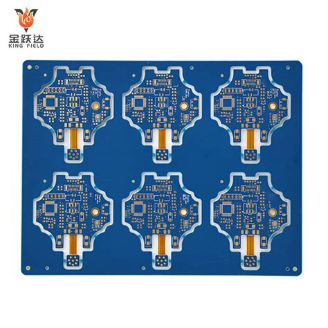
In high-volume PCB manufacturing business models, standardized panel utilization strategies—such as nesting irregularly shaped boards—lower material costs by up to 18%. Always align your layout with the flex circuit’s bend-to-install or dynamic flexing requirements; misjudging these can lead to premature fatigue. By combining space-saving layouts with rigorous simulation testing, you achieve durable, lightweight designs that meet both performance and economic benchmarks.

Lightweight Flex Circuit Design Principles
When designing lightweight flex circuits, you must balance structural integrity with weight reduction—a critical factor in aerospace, wearables, and portable electronics. Start by selecting ultra-thin polyimide substrates (25-50µm) paired with rolled annealed copper, which maintains flexibility while minimizing mass. PCB manufacturing companies often prioritize these materials for high-reliability applications, as they withstand repeated bending without cracking.
To optimize weight, analyze trace geometries: narrower conductors (75-100µm) and reduced spacing (50-75µm) lower copper usage without compromising electrical performance. This approach directly impacts PCB manufacturing cost by minimizing raw material waste. For multi-layer designs, consider staggered vias and adhesive-free bonding techniques to eliminate unnecessary dielectric layers—key strategies in PCB manufacturing business models focused on compact, high-density solutions.
Dynamic applications demand attention to mechanical stress distribution. Use finite element analysis (FEA) tools to simulate bend cycles and identify failure-prone areas. Reinforce transition zones with tapered stiffeners or selective stiffening materials, ensuring compliance with bend radius limits. Partnering with PCB manufacturing specialists ensures your design aligns with fabrication capabilities, avoiding costly reworks.
Finally, integrate lightweight components like chip-scale packages (CSPs) and thin-film resistors. These not only reduce overall mass but also enable space-efficient layouts—a priority for industries where every gram counts. By harmonizing material choices, geometric optimization, and collaborative prototyping, you create flex circuits that excel in both performance and manufacturability.
Durable Flex PCB Fabrication Methods
When designing durable flex circuits, you must prioritize material resilience and PCB manufacturing processes that withstand repeated bending and environmental stressors. Start by selecting high-performance substrates like polyimide films, which offer superior thermal stability and mechanical endurance compared to standard materials. Top-tier PCB manufacturing companies often combine these films with rolled annealed (RA) copper, balancing flexibility and conductivity while minimizing fatigue cracks.
Adhesive systems also play a critical role—opt for acrylic or epoxy-free bonding layers to reduce delamination risks during dynamic flexing. For applications in harsh environments, consider adding protective coatings such as solder mask or silicone overlays to shield circuits from moisture, chemicals, or abrasion.
To manage PCB manufacturing cost without compromising durability, refine your layer stack-up. Fewer layers reduce complexity, but strategic placement of stiffeners in high-stress areas (e.g., connector junctions) enhances longevity. Advanced etching techniques, like laser ablation, ensure precise trace geometries, preventing weak points that could fail under cyclic loads.
Finally, collaborate closely with your PCB manufacturing business partner to validate designs through accelerated life testing. Simulations like bend-cycle analysis or thermal shock tests help identify failure modes early, ensuring your flex boards meet industry standards for ruggedized electronics. By balancing material science and process innovation, you create circuits that endure without sacrificing performance.

Flex PCB Material Optimization Techniques
When optimizing materials for flexible circuits, you need to balance mechanical resilience with electrical performance. Start by selecting polyimide films with optimal thermal stability—these withstand repeated bending while maintaining dielectric integrity. For dynamic applications, prioritize adhesiveless laminates to eliminate delamination risks, a common failure point in PCB manufacturing.
Thinner copper layers (≤12µm) reduce stiffness, enhancing bend endurance without compromising conductivity. Pair this with low-loss substrates like liquid crystal polymer (LCP) for high-frequency applications, where signal integrity is critical. PCB manufacturing companies often recommend hybrid constructions—combining rigid sections for component support and flexible zones for movement—to minimize PCB manufacturing cost while maximizing reliability.
Material choices directly impact durability. For instance, coverlays with acrylic adhesives offer better moisture resistance than epoxy alternatives, crucial for harsh environments. When sourcing, verify suppliers provide certified flex-grade materials—subpar options may crack under cyclic stress, escalating long-term PCB manufacturing business expenses. Finally, collaborate with fabricators early to align material specs with your design’s mechanical demands, ensuring seamless integration into complex assemblies.

Harsh Environment Flex PCB Design
When designing flex circuits for harsh environments, you must prioritize durability alongside electrical performance. PCB manufacturing companies face unique challenges in balancing PCB manufacturing cost with the need for specialized materials that withstand extreme temperatures, moisture, or chemical exposure. Start by selecting substrates like polyimide or liquid crystal polymer (LCP), which offer inherent resistance to thermal cycling and corrosion. For applications like aerospace or industrial sensors, reinforcing critical areas with stiffeners or adhesive systems prevents delamination under mechanical stress.
Transitioning from design to production requires collaboration with PCB manufacturing experts to validate material compatibility with your operating conditions. For instance, dynamic flexing zones may need additional conformal coatings to protect against abrasion, while static regions benefit from thicker copper layers for heat dissipation. Optimizing PCB manufacturing business workflows—such as laser drilling for precise via formation—ensures reliability without inflating costs. Always validate designs through accelerated life testing, simulating environmental stressors like humidity or vibration to identify failure points before mass production. By aligning material choices, protective strategies, and fabrication processes, you create robust flex circuits that thrive where rigid boards fail.
Flex-Rigid Transition Zone Design Strategies
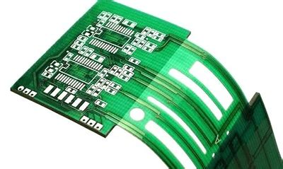
When designing flex-rigid PCBs, the transition zones between rigid and flexible sections demand precise engineering to prevent mechanical failure. You must account for stress concentration at these interfaces, which often leads to cracks or delamination under repeated bending. To mitigate this, stagger the termination points of rigid-section copper layers and use tapered flex-to-rigid transitions to distribute forces evenly. PCB manufacturing companies typically recommend maintaining a minimum unsupported flex length (5-10x the material thickness) near transition areas to avoid abrupt bending.
Material compatibility is equally critical—match the coefficient of thermal expansion (CTE) between rigid and flex layers to prevent warping during thermal cycling. Adhesives with high peel strength, such as acrylic-based systems, enhance bond durability in these zones. When optimizing PCB manufacturing cost, consider using hybrid stack-ups with polyimide flex cores and FR-4 rigid sections, balancing performance and affordability. For high-reliability applications in the PCB manufacturing business, laser-drilled microvias can replace plated through-holes in transition regions, reducing mechanical strain while maintaining signal integrity.
Always validate designs through finite element analysis (FEA) simulations to identify stress hotspots before prototyping. This proactive approach ensures compliance with industry standards while minimizing rework—a key factor in controlling PCB manufacturing timelines and budgets.
Conclusion
Successful PCB manufacturing relies on balancing technical precision with strategic material and design choices. When finalizing flexible circuit designs, you must ensure that dynamic flexing requirements align with PCB manufacturing cost considerations—opting for polyimide or liquid crystal polymer (LCP) substrates, for example, can reduce long-term wear while maintaining budget efficiency. Reputable PCB manufacturing companies often recommend adhering to minimum bend radius guidelines during layout planning to prevent conductor fatigue, a critical factor in harsh environments.
By implementing space-saving layouts and optimizing layer stacking, you can achieve lightweight designs without compromising durability—a priority for industries like aerospace or medical devices. Transition zones in flex-rigid designs demand careful attention to stress distribution, which impacts both reliability and PCB manufacturing business timelines. Collaborating with experienced manufacturers ensures material compatibility and process scalability, particularly when integrating advanced finishes like ENIG or immersion silver.
Ultimately, whether you’re refining thermal management strategies or selecting adhesives for multilayer builds, every decision cascades into the final product’s performance. This approach not only extends operational lifespans but also positions your projects competitively in markets where precision and adaptability define success.
Frequently Asked Questions
How do you calculate the minimum bend radius for dynamic flex circuits?
To determine the minimum bend radius, multiply the total board thickness by 6–10x, depending on material flexibility. Partnering with experienced PCB manufacturing companies ensures adherence to bend radius guidelines, preventing copper cracking during repeated flexing.
What materials optimize durability in harsh environments?
Polyimide substrates paired with acrylic adhesives offer superior thermal stability and moisture resistance. For extreme conditions, consider hybrid materials tested by PCB manufacturing specialists to balance cost and performance.
How does stackup design affect PCB manufacturing cost?
Simplified layer counts and standardized materials reduce expenses, but complex layouts may require advanced processes. Work with your PCB manufacturing business to analyze trade-offs between space-saving designs and fabrication complexity.
Can rigid-flex transition zones improve reliability?
Yes. Gradual tapering of rigid sections and staggered plating in transition zones minimize stress concentrations. Reputable PCB manufacturing providers use finite element analysis (FEA) simulations to validate these designs.
What factors influence lightweight flex circuit performance?
Thin copper foils (≤12µm) and low-mass dielectrics reduce weight while maintaining conductivity. Discuss material thinning limits with your PCB manufacturing partner to avoid compromising signal integrity.
Need Expert Guidance for Your Flex PCB Project?
For tailored solutions in PCB manufacturing, including cost-optimized dynamic flex designs, please click here to consult our engineering team.


