Advanced Heavy Copper PCB Solutions for Enhanced Current Capacity
Key Takeaways
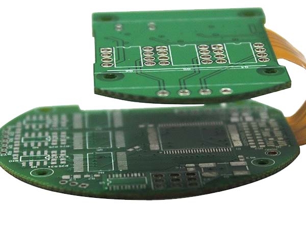
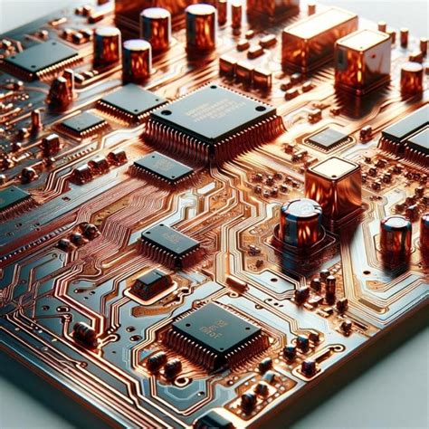
When exploring PCB manufacturing for high-current applications, understanding the role of heavy copper PCBs is critical. These specialized boards, with copper weights ranging from 4–20 oz/ft², outperform standard 1–3 oz PCBs in power electronics by enabling higher current loads and improved thermal stability. PCB manufacturing companies often prioritize advanced etching and plating techniques to maintain structural integrity, as thicker copper layers demand precision to avoid undercutting or delamination.
Tip: When selecting a manufacturer, verify their expertise in heavy copper PCB fabrication—look for certifications like IPC-6012 Class 3 to ensure reliability under extreme conditions.
While PCB manufacturing cost increases with copper weight due to material and processing complexities, the long-term benefits in heat dissipation and durability often justify the investment. For businesses in the PCB manufacturing business, balancing cost with performance requires optimizing designs—for example, using hybrid constructions (combining standard and heavy copper layers) to reduce expenses without sacrificing functionality.
Transitioning from standard to heavy copper designs? Collaborate early with your supplier to address challenges like thermal expansion mismatches or impedance control. For deeper insights into thermal management strategies, review this industry guide. By aligning your requirements with a manufacturer’s capabilities, you can achieve robust solutions tailored to high-power applications like automotive systems or renewable energy infrastructure.
Heavy Copper PCB Power Electronics Benefits
When designing power electronics, you require circuits that handle high-current density without compromising reliability. PCB manufacturing processes for heavy copper boards (4-20 oz/ft²) enable precisely this by embedding thicker conductive layers, directly enhancing current-carrying capacity by up to 5x compared to standard 1-3 oz boards. This capability is critical for applications like EV charging systems or industrial motor drives, where sustained high-power delivery is non-negotiable.
Beyond electrical performance, these boards excel in thermal management. The increased copper mass acts as a built-in heatsink, reducing hotspot formation and extending component lifespan. For pcb manufacturing companies, achieving this requires specialized etching and plating techniques to maintain precise trace geometry despite thicker copper layers—a process that impacts pcb manufacturing cost but delivers unmatched durability.
| Feature | Heavy Copper PCB (4-20 oz) | Standard PCB (1-3 oz) |
|---|---|---|
| Current Capacity | 50-200A+ | 10-30A |
| Thermal Resistance | <1.5°C/W | 3-5°C/W |
| Typical Applications | Power converters, UPS | Consumer electronics |
Leading pcb manufacturing business providers optimize designs for mechanical stability, ensuring plated through-holes and vias withstand repeated thermal cycling. While pcb manufacturing cost rises with copper weight, the long-term savings from reduced failure rates and higher efficiency often justify the investment—especially in mission-critical systems.
4-20 oz/ft Copper PCB Specifications Guide
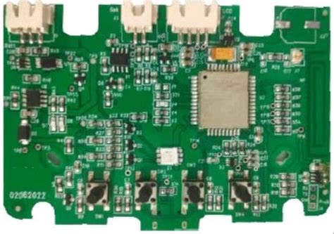
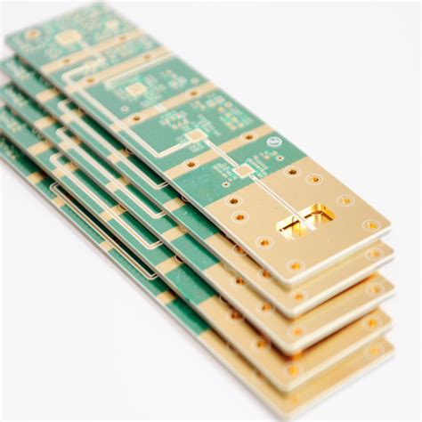
When designing circuits for high-current applications, understanding PCB manufacturing specifications for heavy copper boards becomes critical. Unlike standard 1-3 oz/ft² designs, heavy copper PCB manufacturing companies utilize 4-20 oz/ft² copper weights to handle elevated current loads while minimizing resistive losses. These thicker copper layers enable enhanced conductivity and improved thermal dissipation, making them ideal for power electronics, industrial equipment, or renewable energy systems.
To achieve optimal performance, you must align your design with specific copper weight tolerances. For instance, 4-6 oz/ft² boards suit moderate power demands, while 10-20 oz/ft² variants address extreme current requirements. However, higher copper weights increase PCB manufacturing cost due to specialized etching processes and material handling. Manufacturers often employ controlled-depth milling or step plating to maintain trace integrity, ensuring minimal undercutting during fabrication.
When evaluating PCB manufacturing business partners, verify their capability to manage thicker dielectric materials and multilayer stack-ups. Thermal stress testing and cross-sectional analysis are essential to confirm adherence to IPC-2221B standards. By balancing copper weight, layer configuration, and thermal management strategies, you can optimize both performance and cost-efficiency in high-power designs. This foundational knowledge prepares you to explore advanced optimization strategies in subsequent sections.
High-Current PCB Design Optimization Strategies
When designing high-current PCBs, you must prioritize trace width, copper weight, and thermal pathways to ensure reliable performance. Start by selecting 4-20 oz/ft² copper layers to handle elevated current loads without excessive temperature rise. PCB manufacturing companies specializing in heavy copper boards often recommend widening traces proportionally to current levels—a critical step often overlooked in standard designs. For instance, a 10 oz/ft² copper layer may require trace widths 3-4× larger than those used in 1 oz boards to maintain safe current density.
Integrating thermal vias near high-heat components helps distribute energy efficiently, reducing localized hotspots. Advanced simulation tools can model current flow and heat distribution, enabling you to refine layouts before prototyping—a cost-saving measure that lowers PCB manufacturing cost by minimizing trial runs. Partnering with experienced PCB manufacturing providers ensures access to precision etching techniques, which are vital for maintaining consistent copper thickness in complex designs.
Material selection also plays a role: high-Tg substrates and thermally conductive dielectrics complement heavy copper’s capabilities. While PCB manufacturing business standards vary, prioritize suppliers adhering to IPC-2221A guidelines for current-carrying capacity calculations. Balancing these factors not only enhances reliability but also extends the lifespan of power electronics, making your design choices critical to long-term performance in applications like motor drives or renewable energy systems.
Thermal Management Solutions for Heavy Copper
When designing high-current systems, effective thermal management becomes critical to maintaining PCB manufacturing reliability. Heavy copper PCBs inherently handle higher temperatures due to their thicker conductive layers, but advanced solutions like thermal vias, copper pours, and heatsink integration further enhance heat dissipation. Leading PCB manufacturing companies employ specialized techniques such as staggered via patterns and optimized copper distribution to minimize thermal resistance across the board. While these strategies may increase PCB manufacturing cost initially, they prevent overheating-related failures that could lead to costly redesigns or replacements.
You’ll find that combining high-thermal-conductivity substrates with precision-etched heavy copper layers creates a balanced approach for managing energy density in power electronics. This synergy between material science and fabrication expertise ensures your design meets both current capacity requirements and long-term durability benchmarks – key factors when selecting partners in the PCB manufacturing business. By prioritizing thermal performance early in the design phase, you avoid compromises that could undermine the current-carrying capacity or thermal stability of your application.
Heavy Copper vs Standard PCB Performance
When evaluating PCB manufacturing options for power electronics, understanding performance differences between heavy copper and standard boards becomes crucial. While traditional 1-3 oz/ft² PCBs suffice for low-current applications, designs requiring current densities above 30A/cm² often demand thicker 4-20 oz/ft² copper layers. The increased conductor cross-section in heavy copper boards reduces resistive losses by up to 60% compared to standard equivalents, directly impacting thermal management and long-term reliability.
PCB manufacturing companies specializing in heavy copper solutions optimize trace geometries to prevent localized heating—a common failure point in high-power circuits. This structural advantage enables sustained operation at temperatures exceeding 150°C without performance degradation, whereas standard boards typically derate above 105°C. However, the enhanced capabilities come with elevated PCB manufacturing cost, as thicker copper requires specialized etching processes and longer plating cycles.
For businesses weighing PCB manufacturing business decisions, the performance trade-offs center on application requirements. Heavy copper’s superior heat dissipation eliminates need for supplemental cooling in many cases, offsetting initial cost premiums through reduced system complexity. Standard PCBs remain viable for low-power scenarios, but their thinner conductive layers struggle with thermal cycling stresses in power electronics—a limitation that accelerates material fatigue in demanding environments.
Heavy Copper PCB Manufacturing Quality Standards
When evaluating PCB manufacturing partners for heavy copper boards, you need to verify compliance with industry-recognized certifications like IPC-6012 Class 3 and UL standards. These benchmarks ensure traceability, material integrity, and process consistency—critical for boards handling 4-20 oz/ft² copper weights. Reputable PCB manufacturing companies implement rigorous controls, from copper foil bonding strength tests to plating thickness verification, to prevent delamination or current leakage in high-stress environments.
Advanced PCB manufacturing workflows incorporate laser direct imaging (LDI) for precise circuit patterning and step plating techniques to achieve uniform copper distribution across layers. Such precision reduces PCB manufacturing cost risks associated with rework or field failures. Quality-focused suppliers also perform thermal cycle testing (-55°C to 150°C) and microsection analysis to validate copper integrity under extreme operating conditions.
For your PCB manufacturing business case, prioritize vendors offering real-time process monitoring and material traceability systems. These features ensure adherence to high-current design specifications while balancing performance requirements with budget constraints. Always request cross-sectional reports and electrical test data to confirm compliance with your application’s current-carrying and thermal demands.
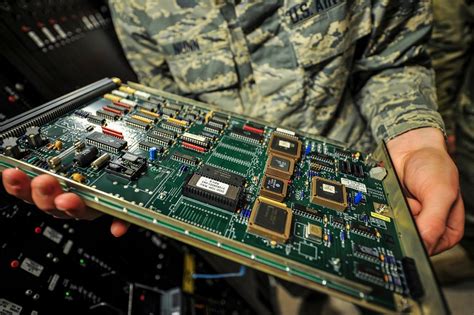
Applications Requiring Enhanced Current Capacity
When designing systems that demand high-current handling, you’ll find standard PCB manufacturing approaches often fall short. Applications like power converters, motor controllers, and automotive battery management systems require traces capable of carrying currents exceeding 100A. This is where heavy copper PCBs (4-20 oz/ft²) become essential, enabling reliable power distribution without risking trace burnout or voltage drops.
PCB manufacturing companies specializing in thick copper designs optimize layer stacking and trace geometries to balance PCB manufacturing cost with performance. For instance, industrial welding equipment and renewable energy inverters leverage these boards to manage extreme thermal stress while maintaining operational stability. By collaborating with experienced PCB manufacturing business partners, you ensure designs meet stringent safety standards for aerospace avionics or medical imaging devices, where failure isn’t an option.
Additionally, heavy copper’s superior heat dissipation reduces reliance on external cooling systems, making it ideal for compact EV charging stations or data center power supplies. As you explore solutions for high-current needs, prioritizing manufacturers with expertise in advanced copper weights ensures your application’s longevity and efficiency.
Thick Copper PCB Advantages for Heat Dissipation
When designing circuits for high-power applications, managing heat effectively becomes critical to ensuring long-term reliability. Thick copper layers (4-20 oz/ft²) in PCBs act as natural heat spreaders, reducing localized hotspots by distributing thermal energy across the board. Unlike standard 1-3 oz copper designs, these heavy-copper boards lower electrical resistance, which directly minimizes parasitic heat generation during high-current operation. By leveraging copper’s inherent thermal conductivity, these boards dissipate heat up to 10x faster than conventional alternatives, reducing reliance on external cooling systems.
For PCB manufacturing companies, achieving optimal thermal performance requires precise control over copper distribution and plating processes. Advanced techniques like embedded thermal vias or hybrid stack-ups further enhance heat transfer efficiency. When working with heavy copper designs, you’ll notice that PCB manufacturing cost may increase due to specialized materials and extended etching times. However, the trade-off pays dividends in applications like industrial motor drives or renewable energy systems, where overheating risks can lead to catastrophic failures.
PCB manufacturing business standards demand rigorous testing for thermal cycling resistance, ensuring boards withstand repeated expansion and contraction. For businesses in power electronics, prioritizing thick copper PCBs isn’t just about handling higher currents—it’s about building systems that outlast competitors through superior thermal management.
Conclusion
When selecting PCB manufacturing companies for high-current applications, it’s critical to prioritize expertise in heavy copper PCB manufacturing. These specialized designs, ranging from 4-20 oz/ft² copper weights, require advanced fabrication techniques to ensure reliability under extreme thermal and electrical stress. While PCB manufacturing costs may initially appear higher compared to standard boards, the long-term benefits—such as reduced failure rates and enhanced durability—often justify the investment, particularly in industries like power electronics or automotive systems.
To optimize your PCB manufacturing business outcomes, collaborate with partners who adhere to rigorous quality standards and offer tailored solutions for thick copper designs. This ensures your final product not only meets but exceeds performance expectations, balancing thermal management with current-carrying capacity. By aligning your design goals with a manufacturer’s technical capabilities, you secure a competitive edge in markets demanding robust, high-performance circuitry.
FAQs
How does heavy copper PCB manufacturing differ from standard processes?
PCB manufacturing for heavy copper requires specialized plating and etching techniques to handle 4-20 oz/ft² copper weights. Unlike standard 1-3 oz boards, these processes ensure precise current handling while maintaining structural integrity.
What factors influence PCB manufacturing costs for heavy copper designs?
PCB manufacturing cost increases with copper weight due to extended processing times, advanced materials, and stricter quality controls. However, the enhanced durability and thermal performance justify the investment for high-current applications like power electronics.
How do you select reliable PCB manufacturing companies for heavy copper boards?
Look for PCB manufacturing companies with certifications like IPC Class 3 and proven expertise in thick copper fabrication. Review their portfolio for similar projects and ensure they offer design support to optimize current density and heat dissipation.
Can heavy copper PCBs reduce long-term operational costs?
Yes. By minimizing thermal stress and improving reliability, these boards lower maintenance needs and downtime, offering better ROI for PCB manufacturing business clients in industrial or automotive sectors.
What industries benefit most from heavy copper PCB solutions?
Applications requiring enhanced current capacity—such as renewable energy systems, EV charging stations, and aerospace controls—rely on heavy copper PCBs for their ability to sustain high power loads without overheating.
Ready to Optimize Your High-Current Designs?
For tailored heavy copper PCB solutions, please click here to connect with experts at Andwin PCB. Ensure your project meets the highest PCB manufacturing quality standards while balancing performance and cost.