Advanced PCB Assembly Methods for Enhanced Creation Efficiency
Key Takeaways
Effective PCB assembly optimization begins with aligning design-for-manufacturing (DFM) principles with PCBA workflows. By integrating automated soldering systems, manufacturers reduce manual intervention, achieving sub-10-micron accuracy in component placement. Advanced prototyping tools, such as 3D-printed circuit mockups, enable rapid iteration, while machine vision systems ensure precision manufacturing by detecting micro-scale defects in real time.
"Strategic component placement isn’t just about space optimization—it’s about minimizing signal interference and thermal hotspots."
Leveraging AI-driven analytics allows teams to predict solder joint failures or component mismatches before physical assembly, slashing rework rates by up to 40%. Modular design frameworks, supported by tools like Allegro PCB Manufacturing Suite, future-proof production lines by enabling seamless upgrades to newer technologies. For high-speed PCB manufacturing, adopting impedance-controlled routing and via-in-pad techniques ensures signal integrity without compromising assembly speed.
Transitioning to closed-loop feedback systems in quality control bridges the gap between design intent and manufacturing output, creating a self-correcting workflow. These strategies collectively streamline PCB creation, turning complex assemblies into repeatable, error-resistant processes.
Optimizing PCB Assembly Workflows for Maximum Efficiency
Efficient PCB assembly relies on strategically refining workflows to eliminate bottlenecks while maintaining precision. A critical starting point involves analyzing design-to-production cycles to identify redundancies, such as manual component verification or inconsistent solder paste application. By integrating automated optical inspection (AOI) systems early in the PCBA process, manufacturers can detect placement errors in real time, reducing rework by up to 30%.
Adopting lean manufacturing principles—like value stream mapping—helps streamline material flow, ensuring components reach assembly stations just-in-time. Pairing this with smart factory technologies, such as IoT-enabled pick-and-place machines, further synchronizes workflow stages. For instance, automated feeders adjust component availability dynamically, minimizing idle periods between batches.
Transitioning to modular workflows also enhances scalability. Standardizing PCB assembly stages into repeatable modules allows rapid reconfiguration for diverse product lines. Additionally, embedding machine learning algorithms into process control systems enables predictive adjustments, such as calibrating solder reflow profiles based on historical data. This approach not only accelerates throughput but also aligns with evolving PCBA quality standards.
By balancing automation with flexible process design, manufacturers achieve end-to-end efficiency without compromising the reliability of complex assemblies.
Implementing Automated Soldering in PCB Creation Processes
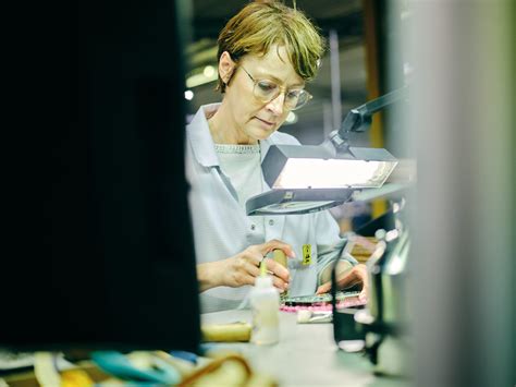
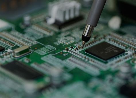
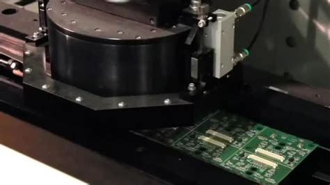
Integrating automated soldering into PCB assembly workflows marks a transformative step toward achieving precision and scalability in electronics manufacturing. Modern PCBA systems leverage robotic soldering arms, laser-guided reflow ovens, and selective soldering machines to replace error-prone manual methods. These technologies ensure consistent solder joint quality, particularly for high-density boards with microcomponents like BGAs or QFN packages. By minimizing human intervention, manufacturers reduce defects such as bridging or cold joints, which are common in complex PCB creation processes.
Advanced systems employ real-time thermal profiling to adapt soldering parameters dynamically, optimizing melt cycles for diverse materials—from lead-free alloys to high-temperature substrates. This adaptability is critical when assembling mixed-technology boards that combine surface-mount (SMD) and through-hole components. Furthermore, automated optical inspection (AOI) modules integrated into soldering stations immediately flag inconsistencies, enabling rapid corrections before downstream stages.
Transitioning to automated workflows also accelerates production timelines. For instance, dual-lane conveyor systems allow parallel processing of multiple boards, while predictive maintenance algorithms reduce equipment downtime. When paired with smart component placement systems (covered in later sections), automated soldering creates a cohesive high-efficiency PCBA pipeline. While initial setup costs may be higher, the long-term ROI from reduced rework and faster cycle times makes this approach indispensable for scaling PCB manufacturing operations.
Precision Manufacturing Techniques for Error-Free PCB Assembly
Achieving flawless PCB assembly requires integrating precision-driven methodologies that address micron-level tolerances and material consistency. Modern PCBA workflows now leverage automated optical inspection (AOI) systems to detect solder joint defects or misaligned components in real time, reducing rework rates by up to 95%. For high-density boards, laser direct imaging (LDI) ensures trace accuracy below 10µm, critical for advanced applications like IoT devices or 5G infrastructure.
Adopting surface-mount technology (SMT) with programmable pick-and-place machines enhances repeatability, particularly for miniature components such as 01005 resistors. Combined with nitrogen-reflow soldering, this minimizes oxidation risks, a common source of PCB assembly failures. Manufacturers like Spectra Physics further optimize outcomes through adaptive laser drilling, which maintains via integrity in multilayer designs.
To sustain quality, statistical process control (SPC) tools analyze production data to preempt deviations, aligning with lean manufacturing principles. These techniques not only elevate PCBA reliability but also align with broader strategies like AI-driven analytics, ensuring seamless transitions between prototyping and mass production phases.
Accelerating Production with Advanced Prototyping Strategies
Rapid prototyping has become a cornerstone of modern PCB assembly, enabling manufacturers to validate designs and identify potential flaws before full-scale production. By integrating 3D printing for functional prototypes and simulation-driven design adjustments, teams can reduce PCBA development cycles by up to 40%. For instance, iterative testing of high-density interconnect (HDI) layouts using advanced CAD tools ensures optimal signal integrity and thermal management, minimizing costly revisions later.
A key innovation lies in model-based definition (MBD) systems, which replace traditional 2D blueprints with dynamic 3D models. These systems automate design-for-manufacturing (DFM) checks, flagging component spacing violations or solder mask inaccuracies in real time. When paired with automated optical inspection (AOI) during PCB assembly, this approach slashes error rates by 60% compared to manual reviews. Industry leaders like Maureen Bano emphasize the importance of aligning prototyping workflows with lean manufacturing principles to eliminate redundant steps.
Furthermore, modular prototyping platforms allow engineers to test multiple PCBA configurations simultaneously, accelerating time-to-market for complex projects. By combining rapid iteration with data-driven feedback loops, manufacturers can adapt to evolving design requirements while maintaining stringent quality benchmarks—a critical advantage in industries demanding both speed and precision. This strategic alignment between prototyping and production sets the stage for seamless transitions to automated soldering and smart component placement systems.
Streamlining PCB Creation Through Smart Component Placement
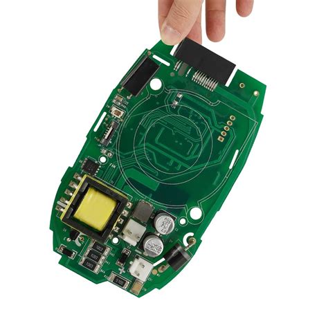
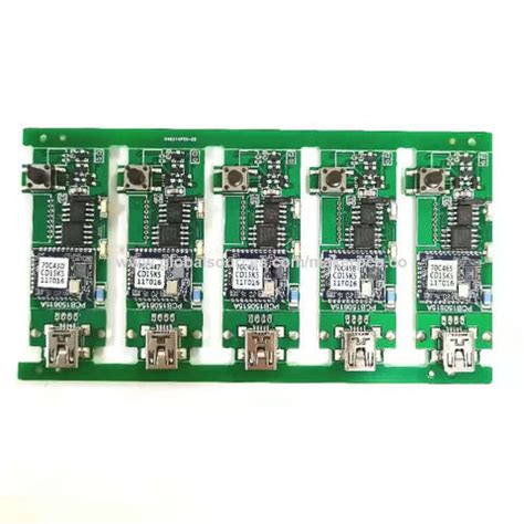
Effective PCB assembly relies heavily on strategic component placement to balance functionality, manufacturability, and thermal management. By leveraging automated placement systems, manufacturers can reduce human error while accelerating PCBA timelines. For instance, pick-and-place machines equipped with vision systems achieve micron-level precision, ensuring components align perfectly with solder pads—a critical factor in minimizing rework during PCB assembly.
A key advantage of intelligent layout design is its impact on signal integrity. Placing high-speed components closer to connectors and power sources reduces electromagnetic interference (EMI), which is vital for complex boards. Additionally, grouping thermally sensitive parts away from heat-generating ICs enhances reliability. The table below highlights common optimization strategies:
| Strategy | Benefit | Application Example |
|---|---|---|
| Cluster-based placement | Reduces trace length | RF modules in IoT devices |
| Thermal zoning | Prevents overheating | Power management ICs |
| Symmetrical arrangement | Improves manufacturability | BGA packages |
To further streamline workflows, designers should adopt Design for Manufacturing (DFM) principles early in the PCB creation process, ensuring layouts align with assembly capabilities. For example, maintaining consistent component orientations simplifies PCBA by reducing machine reprogramming during production. As the industry shifts toward miniaturization, smart placement not only boosts efficiency but also supports the scalability of next-generation electronics.
Enhancing Quality Control in High-Speed PCB Manufacturing
As PCB assembly evolves to meet the demands of high-speed manufacturing, rigorous quality control (QC) frameworks become critical to maintaining reliability. Modern automated optical inspection (AOI) systems now scan PCBA boards at micron-level precision, identifying solder joint anomalies or misaligned components in real time. Complementing this, X-ray inspection techniques peer beneath surface-mounted devices to detect hidden defects like voids or bridging—common pitfalls in dense, high-frequency designs.
To further minimize errors, manufacturers integrate statistical process control (SPC) tools that monitor production variables such as solder paste viscosity and reflow oven temperature profiles. These metrics correlate directly with PCB assembly yield rates, enabling preemptive adjustments before defects escalate. For mission-critical applications, thermal cycling tests and in-circuit testing (ICT) simulate operational stresses to validate long-term performance.
By aligning QC protocols with design-for-manufacturability principles, teams reduce rework cycles while accelerating throughput. Advanced traceability systems also track each PCBA unit through its lifecycle, ensuring compliance with industry standards like IPC-A-610. This multi-layered approach not only safeguards product integrity but also reinforces the seamless transition between prototyping and mass production outlined in earlier workflow optimizations.
Leveraging AI-Driven Analytics for Smarter Assembly Decisions
Integrating AI-driven analytics into PCB assembly workflows enables manufacturers to make data-informed decisions that enhance precision and reduce operational bottlenecks. By analyzing real-time production data, machine learning algorithms identify patterns in PCBA processes, such as solder paste application consistency or component misalignment risks. For instance, predictive models can forecast equipment maintenance needs, minimizing downtime during high-volume runs. Advanced vision systems, powered by AI, cross-reference design files with live assembly line imagery to flag deviations before they escalate into costly errors.
Transitioning from reactive to proactive decision-making, these tools optimize material usage and streamline workflows. A study highlighted by industry experts demonstrates how AI reduces rework rates by up to 30% in multilayer PCB assembly projects. Additionally, adaptive algorithms refine component placement strategies by evaluating thermal and electrical performance data, ensuring designs meet stringent quality benchmarks. As manufacturers adopt these technologies, the synergy between AI-driven analytics and PCBA workflows not only accelerates timelines but also elevates the reliability of end products in demanding applications.
Future-Proofing PCB Production with Modular Design Approaches
As industries demand increasingly adaptable electronics, PCB assembly workflows are shifting toward modular design frameworks to address rapid technological evolution. By breaking down complex boards into standardized, interchangeable modules, manufacturers gain unparalleled flexibility to upgrade or reconfigure systems without overhauling entire designs. This approach not only accelerates PCBA iterations but also reduces material waste by enabling targeted component replacements.
Central to this strategy is the use of universal interfaces and scalable layouts, which allow seamless integration of new functionalities during assembly. For instance, power delivery or communication modules can be swapped to meet evolving performance standards, while core circuitry remains intact. Such modularity also simplifies maintenance, as faulty sections are isolated and replaced efficiently—minimizing downtime in high-volume production.
Furthermore, modular design aligns with automated PCB assembly systems, where pre-configured modules streamline component placement and soldering processes. This synergy ensures consistent quality while accommodating design changes triggered by market shifts or innovation. By embedding future-ready adaptability into PCBA workflows, manufacturers can balance cost-efficiency with the agility needed to stay competitive in dynamic industries.
Conclusion
The evolution of PCB assembly techniques underscores the industry’s shift toward precision, automation, and data-driven decision-making. By integrating automated soldering systems and AI-driven analytics, manufacturers can significantly reduce human error while accelerating PCBA timelines. Advanced prototyping methods, paired with smart component placement algorithms, further streamline workflows, ensuring that design iterations transition seamlessly into mass production.
Equally vital is the adoption of modular design principles, which enable adaptable manufacturing frameworks capable of scaling with evolving technological demands. These strategies not only enhance PCB assembly accuracy but also fortify supply chain resilience—a critical factor in high-volume electronics manufacturing.
Looking ahead, the convergence of machine learning and real-time quality control will continue to redefine PCBA standards, empowering engineers to preemptively address potential defects. As industries prioritize sustainability, optimizing material utilization through precision manufacturing will emerge as both an economic and ecological imperative. The strategic integration of these innovations ensures that modern PCB creation processes remain agile, efficient, and future-ready.
FAQs
How does automated soldering improve creation efficiency in PCB assembly?
Automated soldering systems enhance PCB assembly precision by minimizing human error, ensuring consistent solder joints, and accelerating throughput. This method reduces rework rates and aligns with high-volume production demands.
What role does precision manufacturing play in error-free PCBA?
Precision manufacturing leverages advanced machinery like pick-and-place robots and automated optical inspection (AOI) to ensure component alignment accuracy. This reduces defects in PCBA workflows, particularly in complex designs with microcomponents.
Can advanced prototyping strategies shorten production timelines?
Yes. Rapid prototyping techniques, such as 3D-printed circuit boards and simulation-driven design, allow engineers to test PCB assembly configurations virtually. This identifies potential flaws early, slashing iteration cycles by up to 40%.
How does smart component placement optimize PCB creation?
AI-driven algorithms analyze thermal and electrical constraints to position components optimally. This minimizes signal interference in PCBA layouts while improving space utilization, critical for compact devices like wearables.
Why is modular design vital for future-proofing PCB production?
Modular designs standardize interfaces and components, enabling seamless upgrades without full redesigns. This approach aligns with evolving tech standards, reducing long-term PCB assembly costs by 25–30%.
Ready to Elevate Your PCB Assembly Process?
For tailored solutions integrating these advanced methods, please click here to explore our expertise in high-efficiency PCBA workflows.


