Advanced PCB Assembly Technology Speedy PCB Assembly Pty Ltd
Key Takeaways
Modern PCB assembly processes integrate high-density interconnect technologies and automated optical inspection systems to ensure both speed and accuracy. For PCBA projects requiring rapid turnaround, manufacturers employ surface-mount technology (SMT) alongside advanced pick-and-place systems, reducing manual intervention while maintaining sub-20μm placement precision.
"Optimizing thermal management during PCB assembly is critical for high-power applications—improper heat dissipation can reduce component lifespan by up to 40%."
Below is a comparison of prototyping vs. high-volume production strategies:
| Factor | Prototyping | High-Volume Production |
|---|---|---|
| Lead Time | 24–72 hours | 2–4 weeks |
| Testing Depth | Functional + Environmental | Automated In-Circuit (ICT) |
| Material Flexibility | FR4, Rogers, Flex | Standardized FR4 |
Design-for-manufacturability (DFM) checks remain essential across all stages, with signal integrity analysis preventing 68% of post-production errors. For PCBA workflows, implementing traceability systems ensures compliance with ISO 9001:2015 and IPC-A-610 standards.
Tip: When selecting a PCB assembly partner, verify their capability to handle mixed-technology boards (through-hole + SMT) and ask about their failure mode analysis protocols.
Transitioning from prototype to mass production requires recalibrating automated stencil printers and reflow profiles to maintain ±0.1°C thermal uniformity. This alignment reduces solder defects by 22% in high-volume PCBA runs.
Rapid PCB Prototyping Solutions
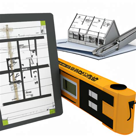
In today’s fast-paced electronics industry, rapid PCB prototyping serves as a critical bridge between design validation and full-scale production. By leveraging advanced PCB assembly techniques, manufacturers like Speedy PCB Assembly Pty Ltd streamline the development cycle, enabling engineers to test and refine designs within days rather than weeks. This acceleration is achieved through automated optical inspection (AOI) systems, which ensure component placement accuracy, and 3D printing technologies for rapid tooling adjustments.
The integration of PCBA (printed circuit board assembly) workflows with agile prototyping processes allows for iterative testing of complex circuits, minimizing design flaws early. For instance, high-frequency signal integrity and thermal management are validated using precision simulation tools before moving to high-volume production. Material selection—such as high-Tg laminates or flexible substrates—is optimized during this phase to meet specific performance requirements.
To maintain competitiveness, Speedy PCB Assembly Pty Ltd employs just-in-time manufacturing principles, reducing lead times without compromising quality. Real-time collaboration with clients ensures design-for-manufacturability (DFM) checks are embedded at every stage, aligning prototypes with end-use conditions. This approach not only accelerates time-to-market but also establishes a foundation for scalable, cost-effective transitions to mass production—a key advantage in sectors like IoT, automotive, and medical devices.
High-Volume PCB Production Strategies
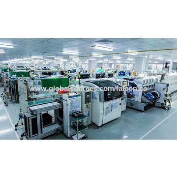
Achieving efficiency in high-volume PCB production demands a strategic balance between speed, scalability, and quality. Modern PCB assembly workflows leverage automated pick-and-place systems and advanced soldering technologies to maintain precision while scaling output. For PCBA (Printed Circuit Board Assembly) projects requiring thousands of units, manufacturers deploy modular production lines that adapt seamlessly to design iterations, minimizing downtime between batches.
A critical component of high-volume success lies in design for manufacturability (DFM) analysis, which identifies potential bottlenecks before mass production begins. By optimizing panel layouts and material selection, PCB assembly teams reduce waste and accelerate throughput. Real-time monitoring systems further enhance yield rates by tracking solder paste application, component alignment, and thermal profiles during reflow processes.
To meet fluctuating demand, leading PCBA providers implement just-in-time inventory management, ensuring component availability without overstocking. This approach, combined with rigorous stress-testing protocols, ensures consistent performance across large batches. Transitioning from prototyping to mass production becomes seamless when manufacturers integrate high-volume strategies early in the product lifecycle, aligning technical capabilities with market timelines.
Precision Engineering in Electronics Assembly
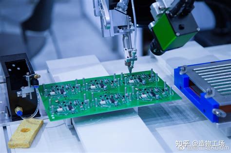
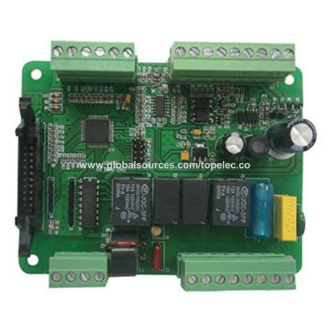
Modern PCB assembly processes demand meticulous attention to detail, where micron-level accuracy ensures reliable performance in complex electronic systems. At the heart of this precision lies advanced PCBA workflows, integrating automated pick-and-place systems, laser-aligned soldering, and multi-stage inspection protocols. These technologies enable consistent placement of surface-mount components, even in high-density designs with pitches below 0.4mm.
Critical to achieving zero-defect outcomes is the synchronization of thermal profiling and material science. Engineers optimize reflow oven parameters to accommodate diverse substrates, from standard FR-4 to flexible polyimide, while mitigating warpage risks in multi-layer boards. Post-assembly, automated optical inspection (AOI) and X-ray imaging verify solder joint integrity, detecting voids or misalignments invisible to the naked eye.
This engineering rigor directly supports downstream phases in electronics manufacturing, ensuring prototypes transition seamlessly to scaled production. By maintaining ±0.1mm positional tolerances across PCBA runs, manufacturers prevent costly rework and accelerate time-to-market—a vital advantage in industries like aerospace and medical devices where component reliability is non-negotiable. As circuit complexity grows, such precision becomes the cornerstone of innovation in next-generation electronic systems.
Advanced PCB Manufacturing Technologies
Modern electronics demand manufacturing processes that balance speed, precision, and scalability. At the core of this evolution lies PCB assembly (PCBA) technology, where innovations like automated surface-mount technology (SMT) and laser-drilled microvias enable sub-millimeter component placement accuracy. These advancements ensure seamless integration of complex circuitry, even in high-density designs.
A critical driver in advanced PCB manufacturing is the adoption of additive processes, such as 3D printed circuitry, which reduces material waste while supporting rapid design iterations. Combined with AI-driven inspection systems, manufacturers achieve near-zero defect rates in PCBA workflows, crucial for aerospace and medical device applications.
Equally transformative is the shift toward flexible hybrid electronics (FHE), merging rigid and flexible substrates to accommodate wearable tech and IoT devices. This approach leverages roll-to-roll processing for mass production without compromising the precision required in PCB assembly.
To maintain competitiveness, leading facilities now integrate real-time data analytics across their PCBA lines, optimizing thermal management during reflow soldering and predicting equipment maintenance needs. Such technologies not only accelerate throughput but also align with global sustainability standards by minimizing energy consumption.
As industries push for smaller, faster, and more reliable devices, the symbiosis of these manufacturing methodologies continues to redefine the boundaries of what’s achievable in electronics production.
Cutting-Edge Electronics Assembly Solutions
Modern electronics manufacturing demands solutions that balance speed, precision, and scalability. PCB assembly processes now incorporate automated optical inspection (AOI) and 3D solder paste inspection (SPI) to ensure micron-level accuracy in component placement. These technologies are critical for PCBA workflows, where even minor deviations can compromise circuit performance. Advanced assembly lines integrate machine learning algorithms to predict and correct potential defects in real time, reducing rework cycles by up to 40%.
For high-complexity designs, flexible printed circuit boards (FPCBs) and rigid-flex hybrids are assembled using laser-assisted alignment systems, enabling seamless integration into compact, high-density devices. Thermal management solutions, such as embedded heat sinks and thermal vias, further enhance reliability in demanding applications like automotive or aerospace systems.
Transitioning from prototyping to mass production, modular PCB assembly platforms allow rapid reconfiguration for varying batch sizes. This adaptability ensures consistent quality across low- and high-volume orders while maintaining compliance with ISO 9001 and IPC-A-610 standards. By leveraging these innovations, manufacturers achieve faster time-to-market without sacrificing the precision required for next-generation electronics.
Speedy PCB Assembly Process Breakdown
The PCB assembly process at Speedy PCB Assembly Pty Ltd integrates automated workflows and precision engineering to ensure efficiency without compromising quality. Beginning with design verification, engineers use advanced software to validate circuit layouts, ensuring compatibility with high-density interconnect (HDI) boards and mixed-technology components. This phase minimizes errors before material procurement, reducing delays in rapid prototyping.
Next, surface-mount technology (SMT) equipment places micro-components onto boards with micron-level accuracy, followed by reflow soldering to establish reliable electrical connections. For complex designs requiring PCBA integration, dual-stage soldering processes accommodate both SMT and through-hole components. Automated optical inspection (AOI) systems then scan assemblies for defects, flagging issues like solder bridging or misaligned parts.
To maintain scalability, the production line employs modular workflows that adapt seamlessly between low-volume prototypes and high-volume PCB production. Real-time data analytics monitor throughput rates, optimizing cycle times while adhering to IPC-A-610 standards. Post-assembly, boards undergo functional testing using customized jigs and burn-in chambers to simulate operational stress.
By combining cutting-edge PCB manufacturing technologies with rigorous process controls, Speedy PCB Assembly Pty Ltd ensures consistent performance across industries—from aerospace to consumer electronics. This structured approach not only accelerates turnaround but aligns with the broader focus on PCB quality control best practices, which will be detailed in subsequent sections.
PCB Quality Control Best Practices
Implementing rigorous PCB assembly quality control protocols ensures reliability in modern electronics manufacturing. Central to this process is automated optical inspection (AOI), which scans for soldering defects, component misalignment, or trace irregularities in PCBA units. Combining AOI with X-ray inspection enhances fault detection in multilayer boards, particularly for hidden connections like ball grid arrays (BGAs).
For high-reliability applications, in-circuit testing (ICT) validates electrical performance by simulating operational conditions, while functional testing replicates end-use scenarios to verify system integration. Statistical process control (SPC) tools analyze production data to preemptively identify deviations, reducing rework rates in PCB assembly workflows.
Material traceability remains critical, with certified suppliers providing documentation for substrates, solder alloys, and components. Adherence to IPC-A-610 standards guarantees acceptability criteria for solder joints and mechanical assembly, particularly in PCBA destined for aerospace or medical devices. Thermal profiling during reflow soldering ensures consistent joint formation, preventing latent failures.
By integrating these methodologies, manufacturers achieve zero-defect output thresholds, balancing speed with precision. This systematic approach not only aligns with advanced PCB manufacturing technologies but also reinforces trust in electronics designed for mission-critical applications.
Innovations in Rapid Circuit Board Assembly
The evolution of PCB assembly technologies has revolutionized how manufacturers balance speed and precision in electronics production. Modern rapid circuit board assembly processes leverage AI-driven inspection systems and automated pick-and-place machinery, enabling PCBA workflows to achieve cycle times reduced by up to 40% compared to traditional methods. A critical innovation lies in modular tooling setups, which allow seamless transitions between prototyping and high-volume runs without compromising accuracy. For instance, laser-direct imaging (LDI) systems now support sub-20μm trace tolerances, ensuring compatibility with ultra-dense IoT and automotive applications.
Another breakthrough involves in-line testing integration, where automated optical inspection (AOI) and functional testing occur simultaneously with soldering, eliminating bottlenecks. Advanced reflow soldering profiles, optimized via machine learning algorithms, further minimize defects in high-speed PCBA environments. Additionally, the adoption of low-temperature co-fired ceramics (LTCC) and high-frequency substrates has expanded design flexibility for 5G and RF circuits. These innovations not only accelerate time-to-market but also align with stringent quality control benchmarks, ensuring reliability even under accelerated production timelines. By merging precision engineering with scalable automation, manufacturers can now meet escalating demands for both rapid prototyping and mass-scale electronics assembly.
Conclusion
The evolution of PCB assembly technologies has redefined modern electronics manufacturing, enabling businesses to meet escalating demands for speed, scalability, and precision. By integrating advanced PCBA methodologies, manufacturers can optimize rapid prototyping cycles while maintaining rigorous quality benchmarks essential for high-volume production. The synergy between automated fabrication processes and data-driven inspection systems ensures that every circuit board aligns with exacting performance specifications, even in complex applications.
As the electronics industry pivots toward miniaturization and IoT integration, the role of precision-driven PCBA workflows becomes increasingly critical. Innovations such as 3D solder paste inspection and AI-assisted defect detection not only enhance reliability but also reduce time-to-market for next-generation devices. For enterprises prioritizing operational excellence, adopting these cutting-edge practices offers a strategic advantage in balancing cost efficiency with uncompromised quality.
Ultimately, the future of electronics manufacturing hinges on continuous advancements in PCB assembly infrastructure, ensuring adaptability to emerging technological paradigms while sustaining the rigorous standards demanded by global markets.
Frequently Asked Questions
What distinguishes standard PCB assembly from PCBA services?
While standard PCB assembly focuses on component placement and soldering, PCBA (Printed Circuit Board Assembly) encompasses full-spectrum services including design validation, automated component sourcing, and functional testing to ensure operational readiness.
How does automated optical inspection enhance PCB assembly quality?
Automated optical inspection (AOI) systems scan boards at micron-level precision, identifying defects like misaligned components or solder bridges. This rigorous quality layer ensures PCBA outputs meet industry-leading reliability standards.
Can Speedy PCB Assembly Pty Ltd handle high-density interconnect (HDI) designs?
Yes, our advanced PCB assembly lines utilize laser-drilled microvias and sequential lamination to support HDI layouts with 0.1mm trace widths, enabling compact, high-performance electronics.
What turnaround times are achievable for prototype PCBA orders?
Rapid prototyping services deliver functional boards in 24-72 hours, leveraging just-in-time material logistics and parallelized production workflows to accelerate development cycles.
How are thermal management challenges addressed in PCB assembly?
Our engineers employ thermal simulation tools and select materials like metal-core substrates or ceramic-filled laminates to optimize heat dissipation in PCBA designs for power electronics.
Explore Customized Solutions for Your Project
For detailed technical specifications or to discuss your PCB assembly requirements, please click here to visit our engineering portal.


