Advanced pcb design
Innovations In High-Density Interconnect (HDI) PCB Design
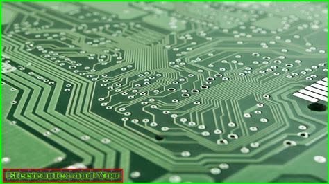
In recent years, the field of printed circuit board (PCB) design has witnessed significant advancements, particularly in the realm of high-density interconnect (HDI) technology. As electronic devices continue to shrink in size while increasing in functionality, the demand for more compact and efficient PCBs has surged.
HDI technology has emerged as a pivotal solution, enabling designers to meet these demands by offering a higher wiring density per unit area compared to traditional PCBs. This innovation is primarily achieved through the use of microvias, finer lines and spaces, and advanced materials, which collectively contribute to the miniaturization and enhanced performance of electronic devices.
One of the most notable innovations in HDI PCB design is the implementation of microvias.
These are small-diameter vias that allow for the interconnection of multiple layers within a PCB. Unlike traditional through-hole vias, microvias occupy less space and enable more complex routing, which is essential for accommodating the increased number of components in modern electronic devices.
The use of microvias not only enhances the electrical performance by reducing signal loss and improving signal integrity but also allows for more efficient use of the available board space. Consequently, designers can incorporate more functionality into a smaller footprint, which is crucial for applications such as smartphones, tablets, and wearable technology.
In addition to microvias, the development of finer lines and spaces has been instrumental in advancing HDI PCB design.
By reducing the width of conductive traces and the spaces between them, designers can increase the density of interconnections on a PCB. This capability is particularly beneficial for high-speed and high-frequency applications, where minimizing signal path lengths and maintaining signal integrity are critical. The advent of laser direct imaging (LDI) technology has further facilitated the production of these finer features, enabling more precise and reliable manufacturing processes. As a result, PCBs can support higher data rates and more complex signal processing, which are essential for modern communication and computing devices.
Moreover, the choice of materials plays a crucial role in the performance and reliability of HDI PCBs.
Advanced materials such as low-loss dielectrics and high-temperature laminates have been developed to meet the stringent requirements of high-speed and high-frequency applications. These materials offer superior thermal and electrical properties, which are essential for maintaining signal integrity and ensuring the longevity of the PCB in demanding environments. Additionally, the use of advanced surface finishes, such as immersion silver and electroless nickel immersion gold (ENIG), provides improved solderability and corrosion resistance, further enhancing the reliability of HDI PCBs.
As the demand for more compact and efficient electronic devices continues to grow, the innovations in HDI PCB design are expected to play an increasingly vital role in the electronics industry.
The integration of microvias, finer lines and spaces, and advanced materials not only addresses the challenges of miniaturization but also paves the way for new possibilities in electronic design. As technology continues to evolve, the ongoing advancements in HDI PCB design will undoubtedly contribute to the development of more powerful, efficient, and versatile electronic devices, ultimately shaping the future of the industry.

The Role Of AI In Optimizing PCB Layouts
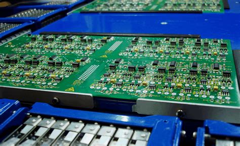
In the rapidly evolving field of electronics, the design and optimization of printed circuit boards (PCBs) have become increasingly complex. As devices become more compact and functionalities expand, the demand for efficient and precise PCB layouts has surged. In this context, artificial intelligence (AI) has emerged as a transformative force, offering innovative solutions to optimize PCB designs. By leveraging AI, engineers can enhance the efficiency, accuracy, and speed of PCB layout processes, ultimately leading to more reliable and cost-effective electronic products.
To begin with, AI algorithms have the capability to analyze vast amounts of data, which is crucial in the PCB design process.
Traditional methods often rely on manual adjustments and iterative testing, which can be time-consuming and prone to human error. In contrast, AI can process complex datasets to identify patterns and correlations that might not be immediately apparent to human designers. This ability allows AI to predict potential design flaws and suggest optimal component placements, thereby reducing the likelihood of errors and improving the overall quality of the PCB layout.
Moreover, AI-driven tools can significantly accelerate the design process.
By automating routine tasks such as routing and component placement, AI enables designers to focus on more strategic aspects of the project. This not only speeds up the development cycle but also allows for more innovative and creative design solutions. For instance, AI can quickly generate multiple design iterations, each optimized for different parameters such as cost, performance, or power consumption. Designers can then evaluate these options and select the most suitable one, thereby streamlining the decision-making process.
In addition to enhancing efficiency, AI also plays a crucial role in optimizing the thermal and electrical performance of PCBs.
As electronic devices become more powerful, managing heat dissipation and signal integrity becomes increasingly challenging. AI algorithms can simulate various thermal and electrical scenarios, providing insights into how different design choices impact performance. This predictive capability allows designers to make informed decisions that enhance the reliability and longevity of the final product.
Furthermore, AI’s role in PCB design extends to the realm of design for manufacturability (DFM).
Ensuring that a PCB design can be efficiently manufactured without defects is a critical consideration. AI can analyze design files to identify potential manufacturing issues, such as insufficient clearances or problematic trace widths, before they become costly problems in production. By addressing these issues early in the design phase, AI helps reduce production costs and improve yield rates.
Despite these advantages, the integration of AI into PCB design is not without challenges.
The complexity of AI models and the need for high-quality training data can pose significant hurdles. Additionally, there is a learning curve associated with adopting AI-driven tools, as designers must become familiar with new software and methodologies. However, as AI technology continues to advance, these challenges are likely to diminish, paving the way for even more sophisticated and user-friendly design solutions.
In conclusion, the role of AI in optimizing PCB layouts is multifaceted and transformative.
By enhancing data analysis, accelerating design processes, improving performance, and ensuring manufacturability, AI is reshaping the landscape of PCB design. As the electronics industry continues to evolve, the integration of AI into PCB design will undoubtedly become increasingly essential, driving innovation and efficiency in the creation of next-generation electronic devices.
Advanced Techniques For Thermal Management In PCB Design
In the realm of advanced printed circuit board (PCB) design, thermal management emerges as a critical consideration, particularly as electronic devices become more compact and powerful. The increasing density of components on PCBs, coupled with higher power consumption, necessitates innovative approaches to dissipate heat effectively. Without proper thermal management, excessive heat can lead to component failure, reduced performance, and decreased reliability. Therefore, understanding and implementing advanced techniques for thermal management is essential for engineers and designers striving to optimize PCB performance.
One of the fundamental strategies in thermal management is the use of thermal vias.
These are small, plated holes that connect the top and bottom layers of a PCB, facilitating the transfer of heat away from critical components. By strategically placing thermal vias beneath heat-generating components, designers can create a more efficient heat dissipation path. This technique is particularly effective in multi-layer PCBs, where heat can be conducted to internal layers and spread over a larger area, thereby reducing localized hotspots.
In addition to thermal vias, the selection of appropriate materials plays a pivotal role in managing heat.
High thermal conductivity materials, such as copper and aluminum, are often used in PCB design to enhance heat dissipation. Copper, in particular, is favored for its excellent thermal and electrical conductivity. By increasing the thickness of copper layers, designers can improve the PCB’s ability to conduct heat away from components. Moreover, incorporating metal core PCBs, which integrate a metal substrate, can further enhance thermal performance by providing a direct path for heat to dissipate.
Another advanced technique involves the use of thermal pads and heat sinks.
Thermal pads are placed between components and the PCB to improve thermal contact and facilitate heat transfer. These pads are typically made from materials with high thermal conductivity, such as silicone or graphite. Heat sinks, on the other hand, are external components attached to the PCB to dissipate heat into the surrounding environment. By increasing the surface area available for heat exchange, heat sinks can significantly reduce the temperature of critical components.
Furthermore, the layout of components on a PCB can greatly influence thermal performance.
By spacing heat-generating components apart and placing them in areas with better airflow, designers can enhance natural convection and reduce the risk of overheating. Additionally, aligning components along the direction of airflow can further improve cooling efficiency. This consideration is particularly important in applications where forced air cooling is employed, such as in high-performance computing systems.
Simulation and modeling tools also play an indispensable role in advanced thermal management.
These tools allow designers to predict thermal behavior and identify potential hotspots before physical prototypes are built. By simulating different scenarios, designers can optimize the placement of components, thermal vias, and heat sinks to achieve the best thermal performance. This proactive approach not only saves time and resources but also ensures that the final product meets the desired thermal specifications.
In conclusion, advanced techniques for thermal management in PCB design are essential for ensuring the reliability and performance of modern electronic devices. By employing strategies such as thermal vias, selecting appropriate materials, utilizing thermal pads and heat sinks, optimizing component layout, and leveraging simulation tools, designers can effectively manage heat dissipation. As electronic devices continue to evolve, the importance of innovative thermal management solutions will only grow, underscoring the need for ongoing research and development in this critical area of PCB design.
Integrating Flexible And Rigid-Flex PCBs In Complex Systems
In the rapidly evolving landscape of electronics, the integration of flexible and rigid-flex printed circuit boards (PCBs) into complex systems has become a pivotal advancement. As electronic devices continue to shrink in size while expanding in functionality, the demand for innovative PCB solutions that can accommodate these changes has surged. Flexible and rigid-flex PCBs offer a unique combination of durability, versatility, and space-saving capabilities, making them ideal for a wide range of applications, from consumer electronics to aerospace systems.
To begin with, flexible PCBs are constructed using materials that allow them to bend and flex without compromising their electrical integrity.
This flexibility enables designers to create circuits that can fit into unconventional shapes and spaces, which is particularly beneficial in devices where space is at a premium. For instance, in wearable technology, flexible PCBs can be seamlessly integrated into clothing or accessories, providing both comfort and functionality. Moreover, their lightweight nature contributes to the overall reduction in device weight, a critical factor in portable electronics.
On the other hand, rigid-flex PCBs combine the best of both worlds by integrating flexible circuits with rigid sections.
This hybrid approach allows for the creation of complex three-dimensional designs that can withstand mechanical stress while maintaining high performance. Rigid-flex PCBs are particularly advantageous in applications where reliability is paramount, such as in medical devices or military equipment. The rigid sections provide structural support and stability, while the flexible parts allow for dynamic movement and connectivity between different components.
The integration of flexible and rigid-flex PCBs into complex systems requires careful consideration of several factors.
One of the primary challenges is ensuring signal integrity across the entire circuit. As signals traverse through different materials and transition between flexible and rigid sections, maintaining consistent electrical performance is crucial. Advanced design techniques, such as impedance matching and careful routing, are employed to mitigate potential issues and ensure optimal functionality.
Furthermore, thermal management is another critical aspect to consider when integrating these PCBs.
The materials used in flexible and rigid-flex PCBs often have different thermal properties compared to traditional rigid boards. Therefore, designers must implement effective heat dissipation strategies to prevent overheating and ensure the longevity of the system. This may involve the use of thermal vias, heat sinks, or other cooling mechanisms tailored to the specific requirements of the application.
In addition to technical considerations, the manufacturing process for flexible and rigid-f
Flex PCBs is inherently more complex than that of traditional rigid boards. The fabrication involves multiple steps, including the precise layering of materials and the careful alignment of flexible and rigid sections. As a result, collaboration with experienced manufacturers who possess the necessary expertise and equipment is essential to achieve high-quality outcomes.
In conclusion, the integration of flexible and rigid-flex PCBs into complex systems represents a significant advancement in PCB design, offering unparalleled versatility and performance. As technology continues to advance, the demand for these innovative solutions is expected to grow, driving further research and development in this field. By addressing the challenges associated with their integration and leveraging their unique benefits, designers can create cutting-edge electronic systems that meet the ever-evolving needs of modern applications.