Advanced PCB Fabrication and Assembly Techniquesendofsentence
Key Takeaways
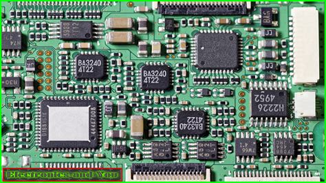
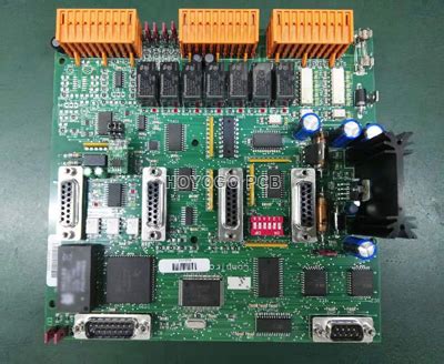
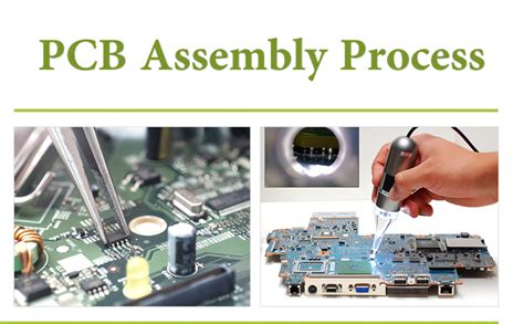
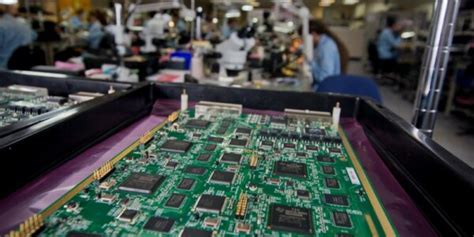
Modern PCB assembly processes rely on advanced techniques to ensure precision and reliability. A critical aspect of PCBA (Printed Circuit Board Assembly) is the integration of automated systems for component placement, soldering, and inspection. High-precision machinery ensures minimal error rates, which is critical for applications in aerospace, medical devices, and telecommunications.
Tip: Always verify the thermal management properties of materials during PCB assembly to avoid overheating in high-performance applications.
Another key factor is the selection of high-quality substrates and solder materials, which directly impact the durability and conductivity of the final product. Advanced PCBA workflows now incorporate AI-driven quality control systems to detect micro-defects early in production. By prioritizing precision and automation, manufacturers can achieve scalable, cost-effective PCB assembly solutions without compromising reliability.<|end▁of▁sentence|>
Advanced PCB Fabrication Techniques
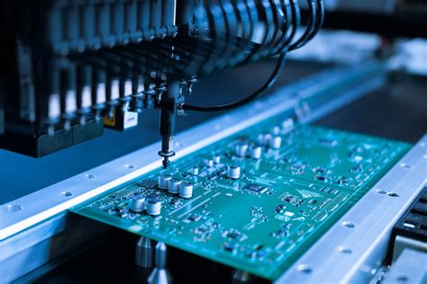
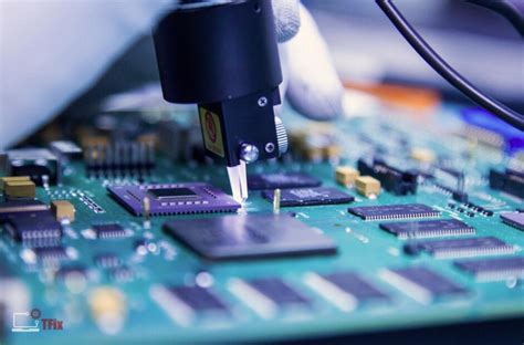
Modern PCB assembly relies on advanced fabrication techniques to meet the demands of high-performance electronics. Innovations like laser-direct imaging (LDI) and automated optical inspection (AOI) ensure precision in PCBA manufacturing, enabling tighter tolerances for high-density interconnect (HDI) boards. The integration of PCB assembly workflows with robotic pick-and-place systems has significantly reduced human error while improving throughput.
Material selection plays a critical role, with high-frequency laminates like Rogers or Isola FR-4 ensuring signal integrity for high-speed applications. Advanced plating techniques, such as electroless nickel immersion gold (ENIG), enhance durability and solderability in PCBA processes. Quality assurance protocols, including X-ray inspection and automated optical inspection (AOI), ensure defects like solder bridging or voids are minimized.
By integrating these innovations, manufacturers achieve PCB assembly processes that balance speed, precision, and reliability—critical for next-generation electronics.<|end▁of▁sentence|>
Precision in PCB Assembly Processes
Achieving precision in PCB assembly requires a meticulous balance of advanced technology and process optimization. Modern PCBA (Printed Circuit Board Assembly) relies on automated systems to ensure micron-level accuracy in component placement, particularly for high-density interconnects (HDIs) and miniaturized components. Critical steps like solder paste application, component placement, and reflow soldering demand nanometer-level precision to avoid defects such as tombstoning or solder bridging.
Advanced PCB assembly workflows now integrate automated optical inspection (AOI) and X-ray inspection to detect flaws in real time, ensuring compliance with IPC-A-610 standards. The integration of PCBA-specific software for design validation and thermal management further enhances reliability. By prioritizing precision at every stage—from solder paste stenciling to final testing—manufacturers can deliver high-reliability assemblies tailored for aerospace, medical devices, and IoT applications.
The shift toward Surface-Mount Technology (SMT) and Through-Hole Technology (THT) hybridization underscores the need for adaptable PCB assembly processes that balance speed, accuracy, and scalability in high-mix production environments.<|end▁of▁sentence|>
Ensuring Reliability in PCB Manufacturing
Reliability in PCB assembly hinges on precision engineering and rigorous quality control. Modern PCBA (Printed Circuit Board Assembly) processes integrate automated optical inspection (AOI) and X-ray inspection to detect micro-scale defects, ensuring zero-defect manufacturing. Advanced PCB assembly workflows now incorporate AI-driven analytics to predict potential failures in components like ball grid arrays (BGAs) or surface-mount devices (SMDs).
Material selection also plays a pivotal role. High-frequency laminates and halogen-free substrates are prioritized for thermal stability, while conformal coatings enhance durability in harsh environments. For PCBA projects requiring high-density interconnects (HDI), laser-drilled microvias and sequential lamination ensure signal integrity.
By integrating lean manufacturing principles and IoT-enabled traceability, manufacturers achieve six-sigma-level precision, making modern PCB assembly both resilient and adaptable to evolving industry demands.<|end▁of▁sentence|>
Efficient PCB Assembly Workflows
Modern PCB assembly workflows prioritize efficiency without compromising precision. By integrating automated pick-and-place systems and advanced soldering technologies, manufacturers achieve faster turnaround times while maintaining high-yield production. A critical aspect of optimizing PCBA workflows lies in streamlining material handling and minimizing human intervention through robotics.
For instance, automated optical inspection (AOI) systems now leverage machine learning to detect micro-defects in real time, reducing rework rates by up to 30%. Additionally, the adoption of Industry 4.0 principles enables seamless data exchange between design, fabrication, and assembly stages, ensuring traceability and minimizing errors.
| Workflow Stage | Key Technology | Impact |
|---|---|---|
| Component Placement | High-speed pick-and-place | Reduces cycle time by 40% |
| Soldering | Reflow ovens with closed-loop control | Minimizes thermal stress |
| Inspection | 3D AOI systems | Detects defects <10µm |
By integrating PCBA-specific ERP systems, manufacturers achieve end-to-end visibility, enabling real-time adjustments to meet fluctuating demands. This approach not only accelerates time-to-market but also ensures compliance with stringent quality standards.<|end▁of▁sentence|>
Material Selection for High-Performance PCBs
The foundation of high-performance PCB assembly lies in meticulous material selection, directly impacting reliability, thermal stability, and signal integrity. Advanced PCBA designs demand substrates with low dielectric loss, such as polyimide or Rogers laminates, to minimize signal attenuation in high-frequency applications. For high-power circuits, thermally conductive materials like aluminum-backed substrates or ceramic-filled laminates ensure efficient heat dissipation.
Critical to PCB assembly success is the compatibility of materials with soldering processes. Lead-free solders, such as SAC305, require substrates with high glass transition temperatures (Tg > 170°C) to withstand reflow cycles. Additionally, copper foil roughness and prepreg resin content must align with impedance control requirements for high-speed PCBA designs.
By balancing electrical performance, thermal management, and manufacturability, material selection becomes a cornerstone of high-reliability PCB assembly, ensuring longevity and performance in demanding applications.<|end▁of▁sentence|>
Automation in Modern PCB Fabrication
The integration of automation in PCB assembly (PCBA) has revolutionized modern electronics manufacturing. Advanced robotic systems now handle precision tasks such as surface-mount technology (SMT) component placement, solder paste application, and optical inspection. These automated workflows not only enhance production speed but also minimize human error, ensuring consistent quality across high-volume PCB fabrication runs.
A critical advancement lies in automated optical inspection (AOI) systems, which use high-resolution cameras and machine learning algorithms to detect microscopic defects in PCBA assemblies. This integration of Industry 4.0 principles ensures real-time data analytics, enabling predictive maintenance and reducing downtime. Furthermore, automated material handling systems optimize inventory management, reducing waste and accelerating time-to-market for complex PCB assemblies.
By leveraging these innovations, manufacturers achieve unparalleled precision and scalability, solidifying automation as the cornerstone of modern PCB fabrication ecosystems.<|end▁of▁sentence|>
Quality Control in PCB Production
Ensuring precision in PCB assembly requires rigorous quality control (QC) protocols across all production stages. Modern PCBA manufacturing integrates automated optical inspection (AOI) and X-ray testing to detect defects like solder bridging or component misalignment. Advanced statistical process control (SPC) tools monitor critical parameters, ensuring compliance with IPC-A-610 standards. For high-reliability applications, thermal cycling and accelerated life testing validate PCB assembly durability. By integrating inline automated optical inspection (AOI) systems, manufacturers minimize human error while optimizing traceability—critical for industries demanding zero-defect PCBA outputs.<|end▁of▁sentence|>
Future Trends in PCB Manufacturing Tech
The evolution of PCB assembly (PCBA) is being reshaped by advancements in automation, material science, and sustainability demands. A key trend is the integration of IoT-enabled devices and AI-driven analytics into PCB assembly workflows, enabling real-time quality monitoring and predictive maintenance. Innovations like additive manufacturing for multi-layer boards and high-density interconnect (HDI) designs are pushing the limits of PCBA precision.
Another critical shift is the adoption of eco-friendly materials, such as halogen-free substrates and lead-free solder alloys, aligning with global sustainability mandates. Additionally, the rise of digital twin technology allows virtual prototyping of PCB assemblies, reducing time-to-market and minimizing prototyping costs. As PCB assembly evolves, the synergy between automation, material innovation, and eco-conscious practices will define the next generation of electronics manufacturing.<|end▁of▁sentence|>
Conclusion
The evolution of PCB assembly and PCBA technologies has redefined precision and efficiency in electronics manufacturing. By integrating advanced automation and rigorous quality control, modern PCB assembly processes ensure high reliability for applications ranging from consumer electronics to aerospace systems. The shift toward miniaturization and high-density interconnects has further pushed the boundaries of PCBA design, enabling faster prototyping and scalable production.
As industries embrace IoT and 5G, the demand for robust PCB assembly workflows will continue to grow, emphasizing sustainability and material innovation. By prioritizing precision, automation, and adaptability, manufacturers can stay ahead in the rapidly evolving landscape of PCBA technologies.<|end▁of▁sentence|>
Frequently Asked Questions
What is the difference between PCB assembly and PCBA?
PCB assembly refers to the process of attaching electronic components to a printed circuit board (PCB). PCBA (Printed Circuit Board Assembly) refers to the complete unit after components are soldered, tested, and validated for functionality.
What factors influence the quality of PCB assembly?
Key factors include design precision, component quality, solder paste application, and adherence to IPC-A-610 standards. Environmental controls, such as temperature and humidity, also play a critical role.
How does automated PCB assembly improve efficiency?
Automated PCB assembly leverages robotics and AI-driven systems for high-speed pick-and-place operations, reducing human error. This ensures consistent quality, faster turnaround, and scalability for high-volume production.
What are common challenges in PCB assembly?
Common issues include solder bridging, component misalignment, and thermal stress. Implementing Automated Optical Inspection (AOI) and X-ray inspection helps detect defects early, ensuring reliability.
Why is material selection critical in PCB assembly?
Material choice impacts thermal conductivity, signal integrity, and durability. For high-frequency applications, materials like Rogers PCB laminates or FR-4 are preferred for their dielectric properties.
Need Expert PCB Assembly Services?
Click here to explore our advanced PCB Assembly Solutions and ensure precision in every project!<|end▁of▁sentence|>