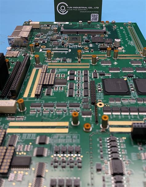
Advanced pcb layout includes high speed layout
Optimizing Signal Integrity in High-Speed PCB Layouts
Optimizing signal integrity in high-speed PCB layouts is a critical aspect of modern electronic design, as the demand for faster and more efficient devices continues to grow. High-speed circuits, which operate at frequencies typically above 50 MHz, are particularly susceptible to signal integrity issues such as crosstalk, electromagnetic interference (EMI), and signal reflection. Therefore, advanced PCB layout techniques must be employed to mitigate these challenges and ensure reliable performance.
One of the fundamental principles in high-speed PCB layout is the careful management of trace impedance.
Impedance mismatches can lead to signal reflections, which degrade signal quality and can cause data errors. To achieve controlled impedance, designers must consider the trace width, the distance between traces, and the dielectric properties of the PCB material. Utilizing tools such as impedance calculators and simulation software can aid in predicting and optimizing trace impedance, thereby enhancing signal integrity.
In addition to impedance control, minimizing crosstalk is essential in high-speed designs.
Crosstalk occurs when a signal on one trace induces an unwanted signal on an adjacent trace, potentially leading to data corruption. To reduce crosstalk, designers should maintain adequate spacing between high-speed traces and employ differential signaling where possible. Differential pairs, which consist of two complementary signals, can significantly reduce susceptibility to crosstalk and EMI by canceling out noise. Furthermore, routing high-speed traces on different layers and using ground planes as shields can further mitigate crosstalk.
Another critical consideration in high-speed PCB layout is the management of power distribution networks (PDNs).
A well-designed PDN ensures that all components receive stable and clean power, which is vital for maintaining signal integrity. Decoupling capacitors play a crucial role in filtering out noise and providing a low-impedance path for high-frequency currents. Placing these capacitors close to the power pins of integrated circuits (ICs) and using multiple capacitors with different values can effectively cover a wide frequency range. Additionally, employing a solid ground plane and minimizing the loop area of power and ground connections can reduce inductive noise and improve overall PDN performance.
Signal integrity can also be enhanced by paying attention to the layout of vias and connectors.
Vias, which are used to connect traces between different layers of the PCB, can introduce impedance discontinuities and signal reflections if not properly designed. To minimize these effects, designers should use vias with controlled impedance and avoid placing them in critical signal paths. Similarly, connectors can be sources of signal degradation if their impedance is not matched to the traces. Selecting high-quality connectors and ensuring proper impedance matching can help maintain signal integrity across the entire PCB.
Thermal management is another aspect that cannot be overlooked in high-speed PCB layouts.
Excessive heat can affect the performance and reliability of electronic components, leading to signal integrity issues. Effective thermal management techniques, such as using thermal vias, heat sinks, and proper component placement, can help dissipate heat and maintain optimal operating conditions.
In conclusion, optimizing signal integrity in high-speed PCB layouts requires a comprehensive approach that addresses various factors, including trace impedance, crosstalk, power distribution, via and connector design, and thermal management. By employing advanced layout techniques and leveraging simulation tools, designers can mitigate signal integrity challenges and ensure the reliable performance of high-speed electronic devices. As technology continues to advance, the importance of meticulous PCB layout design will only grow, making it an indispensable skill for modern electronic engineers.

Techniques for Minimizing Crosstalk in Advanced PCB Designs
In the realm of advanced printed circuit board (PCB) design, minimizing crosstalk is a critical consideration, particularly in high-speed layouts where signal integrity is paramount. Crosstalk, the unwanted coupling of signals between adjacent traces, can lead to significant performance degradation, data corruption, and even complete system failure. Therefore, employing effective techniques to mitigate crosstalk is essential for ensuring the reliability and efficiency of high-speed PCBs.
One fundamental technique for minimizing crosstalk is the strategic placement of traces.
By increasing the spacing between adjacent signal traces, designers can significantly reduce the capacitive and inductive coupling that leads to crosstalk. This approach, while straightforward, requires careful planning and consideration of the available board real estate, especially in densely populated designs. Additionally, maintaining a consistent trace width and spacing throughout the layout can help in achieving uniform impedance, further reducing the potential for crosstalk.
Another effective method involves the use of ground planes.
planes act as a reference point for signals and provide a low-impedance path for return currents, thereby reducing the loop area and minimizing inductive coupling. By placing a continuous ground plane adjacent to signal layers, designers can create a controlled impedance environment that mitigates crosstalk. Moreover, stitching vias can be employed to connect multiple ground planes, ensuring a robust and low-impedance return path across the entire PCB.
Differential signaling is another powerful technique for reducing crosstalk in high-speed PCB designs.
In differential signaling, pairs of traces carry equal and opposite signals, which helps to cancel out any noise or interference picked up along the transmission path. This method not only enhances signal integrity but also improves the overall electromagnetic compatibility (EMC) of the design. To maximize the benefits of differential signaling, it is crucial to maintain tight coupling between the differential pairs and ensure that they are routed symmetrically.
Shielding is also a valuable strategy for crosstalk mitigation.
By placing grounded guard traces or vias between high-speed signal traces, designers can create an effective barrier that prevents unwanted coupling. This technique is particularly useful in scenarios where increasing trace spacing is not feasible due to space constraints. However, it is important to note that improper implementation of shielding can lead to increased parasitic capacitance, which may adversely affect signal integrity. Therefore, careful consideration and simulation are necessary to optimize the placement and effectiveness of shielding elements.
In addition to these physical layout techniques, signal integrity analysis tools play a crucial role in identifying and mitigating crosstalk issues.
Advanced simulation software allows designers to model the PCB layout and predict potential crosstalk problems before the board is fabricated. By analyzing the signal behavior and identifying areas of concern, designers can make informed decisions and implement corrective measures early in the design process. This proactive approach not only saves time and resources but also ensures a higher level of confidence in the final product.
In conclusion, minimizing crosstalk in advanced PCB designs, particularly in high-speed layouts, requires a multifaceted approach that combines strategic trace placement, the use of ground planes, differential signaling, shielding, and thorough signal integrity analysis. By employing these techniques, designers can effectively mitigate crosstalk, ensuring the reliability and performance of their high-speed PCBs. As technology continues to advance and the demand for higher data rates and smaller form factors increases, the importance of mastering these crosstalk mitigation techniques will only grow, making them indispensable tools in the arsenal of modern PCB designers.
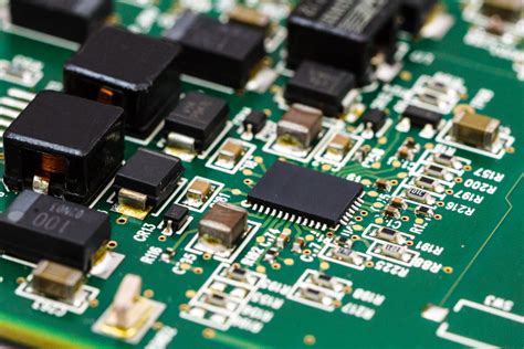
Power Distribution Strategies for High-Speed PCB Layouts
In the realm of advanced printed circuit board (PCB) design, high-speed layouts present unique challenges that necessitate meticulous attention to power distribution strategies. As electronic devices continue to evolve, the demand for faster processing speeds and higher data rates has surged, making efficient power distribution a critical aspect of high-speed PCB layouts. Ensuring stable and reliable power delivery to all components is paramount to maintaining signal integrity and overall system performance.
One of the fundamental principles in power distribution for high-speed PCBs is the implementation of a well-designed power plane.
A power plane, typically a solid copper layer, serves as a low-impedance path for power delivery, minimizing voltage drops and reducing noise. By providing a uniform distribution of power, the power plane helps to maintain consistent voltage levels across the PCB, which is essential for high-speed circuits that are sensitive to voltage fluctuations. Additionally, the power plane acts as a reference plane for signal traces, contributing to improved signal integrity by reducing electromagnetic interference (EMI) and crosstalk.
Transitioning from the concept of power planes, another critical strategy involves the use of decoupling capacitors.
These capacitors are strategically placed near power pins of integrated circuits (ICs) to filter out high-frequency noise and provide instantaneous current to the ICs during switching events. The selection and placement of decoupling capacitors are crucial; they must be chosen based on their frequency response characteristics and positioned as close as possible to the ICs to minimize inductive effects. A combination of capacitors with different values is often employed to cover a broad range of frequencies, ensuring effective noise suppression across the entire spectrum.
Furthermore, the layout of power distribution networks (PDNs) must be carefully planned to avoid common pitfalls such as ground loops and excessive via inductance.
Ground loops, which occur when multiple ground paths create unintended current loops, can introduce noise and degrade signal quality. To mitigate this, designers should ensure a single, continuous ground plane and avoid splitting the ground plane into isolated sections. Similarly, via inductance, which arises from the use of vias to connect different layers of the PCB, can impede high-frequency current flow. Minimizing the number of vias and optimizing their placement can significantly reduce inductive effects and enhance power delivery efficiency.
In addition to these strategies, the use of power integrity simulation tools has become increasingly important in high-speed PCB design.
These tools enable designers to model and analyze the PDN, identifying potential issues such as voltage drops, noise hotspots, and resonances before physical prototyping. By simulating various scenarios and making data-driven adjustments, designers can optimize the PDN for robust performance, reducing the risk of costly revisions and ensuring that the final product meets stringent performance criteria.
Moreover, thermal management is an integral aspect of power distribution in high-speed PCBs.
As power densities increase, effective heat dissipation becomes crucial to prevent overheating and ensure reliable operation. Techniques such as thermal vias, heat sinks, and thermal pads can be employed to enhance heat transfer and maintain optimal operating temperatures. Proper thermal management not only extends the lifespan of components but also contributes to overall system stability.
In conclusion, power distribution strategies for high-speed PCB layouts encompass a range of techniques aimed at ensuring stable and efficient power delivery. From the implementation of power planes and decoupling capacitors to the careful planning of PDNs and the use of simulation tools, each aspect plays a vital role in maintaining signal integrity and system performance. As technology continues to advance, the importance of these strategies will only grow, underscoring the need for meticulous design practices in the pursuit of high-speed excellence.

Best Practices for High-Frequency PCB Layout and Routing
In the realm of advanced printed circuit board (PCB) design, high-frequency layout and routing present unique challenges that require meticulous attention to detail and adherence to best practices. As electronic devices continue to evolve, the demand for high-speed circuits has surged, necessitating a deeper understanding of the principles that govern high-frequency PCB layouts. To ensure optimal performance and reliability, designers must consider several critical factors, including signal integrity, electromagnetic interference (EMI), and thermal management.
One of the foremost considerations in high-frequency PCB design is signal integrity.
At high frequencies, signals are more susceptible to degradation due to factors such as impedance mismatches, crosstalk, and reflections. To mitigate these issues, it is essential to maintain consistent impedance throughout the signal paths. This can be achieved by carefully controlling the trace width, spacing, and the dielectric properties of the PCB material. Additionally, employing differential signaling for high-speed data lines can significantly reduce noise and improve signal integrity by ensuring that any external interference affects both lines equally, thereby canceling out the noise.
Transitioning to the topic of electromagnetic interference, it is crucial to recognize that high-frequency signals can radiate EMI, which can adversely affect the performance of the PCB and nearby electronic devices.
To minimize EMI, designers should implement proper grounding techniques, such as using a solid ground plane. A continuous ground plane not only provides a low-impedance return path for signals but also acts as a shield against EMI. Furthermore, placing decoupling capacitors close to the power pins of integrated circuits can help filter out high-frequency noise, thereby enhancing the overall stability of the circuit.
Thermal management is another vital aspect of high-frequency PCB design.
As the operating frequency increases, so does the power consumption and heat generation. Excessive heat can lead to component failure and reduced lifespan of the PCB. To address this, designers should incorporate thermal vias and heat sinks to dissipate heat effectively. Additionally, selecting materials with high thermal conductivity for the PCB substrate can aid in efficient heat transfer. Proper thermal management ensures that the PCB operates within safe temperature limits, thereby maintaining its performance and reliability.
Moreover, the layout of high-frequency PCBs should be approached with a strategic mindset.
Placing components in close proximity to each other can reduce the length of high-speed signal paths, thereby minimizing signal delay and potential interference. However, it is equally important to avoid placing sensitive analog components near high-speed digital circuits to prevent noise coupling. Utilizing a multi-layer PCB design can also be beneficial, as it allows for the separation of signal, power, and ground planes, thereby reducing crosstalk and improving signal integrity.
In addition to these considerations, simulation and testing play a pivotal role in high-frequency PCB design.
Utilizing advanced simulation tools can help predict potential issues related to signal integrity, EMI, and thermal performance before the physical prototype is built. Post-layout testing, including time-domain reflectometry (TDR) and vector network analysis (VNA), can provide valuable insights into the actual performance of the PCB, allowing for necessary adjustments to be made.
In conclusion, designing high-frequency PCBs requires a comprehensive understanding of various factors that influence signal integrity, EMI, and thermal management. By adhering to best practices such as maintaining consistent impedance, implementing proper grounding techniques, and ensuring effective thermal management, designers can create high-speed circuits that perform reliably and efficiently. The integration of strategic component placement, multi-layer designs, and thorough simulation and testing further enhances the robustness of high-frequency PCB layouts, ultimately leading to superior electronic devices.

