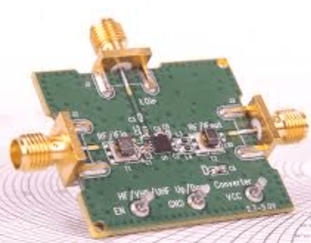
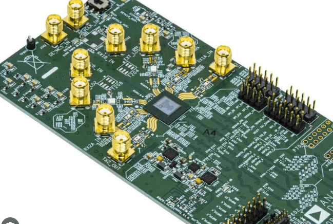
Advanced pcb layout includes high speed layout
Optimizing Signal Integrity in High-Speed PCB Layouts
In the realm of modern electronics, the demand for faster and more efficient devices has led to the evolution of high-speed printed circuit board (PCB) layouts. As the complexity of electronic systems increases, optimizing signal integrity becomes a critical aspect of PCB design. High-speed layouts, characterized by rapid signal transitions and high data rates, present unique challenges that require meticulous attention to detail. To ensure optimal performance, designers must consider various factors that influence signal integrity, including impedance control, crosstalk, and electromagnetic interference (EMI).
One of the fundamental aspects of optimizing signal integrity in high-speed PCB layouts is impedance control.
Impedance mismatches can lead to signal reflections, which degrade signal quality and can cause data errors. To mitigate this, designers must carefully select the appropriate trace widths and spacing, taking into account the dielectric properties of the substrate material. Additionally, the use of controlled impedance traces, such as microstrip or stripline configurations, can help maintain consistent impedance throughout the signal path. By ensuring that the impedance is matched across the entire circuit, signal reflections are minimized, thereby enhancing signal integrity.
In addition to impedance control, managing crosstalk is crucial in high-speed PCB layouts.
Crosstalk occurs when signals on adjacent traces interfere with each other, leading to unwanted noise and potential data corruption. To reduce crosstalk, designers can employ techniques such as increasing the spacing between traces, using ground planes to provide isolation, and routing critical signals on different layers. Furthermore, differential signaling, which involves using pairs of traces to carry signals, can be an effective strategy to minimize crosstalk. By utilizing these methods, designers can ensure that signals remain clean and free from interference, thus preserving signal integrity.
Electromagnetic interference (EMI) is another significant concern in high-speed PCB layouts.
EMI can originate from both internal and external sources, and it can adversely affect the performance of electronic systems. To combat EMI, designers can implement shielding techniques, such as using ground planes and metal enclosures, to contain and isolate electromagnetic fields. Additionally, careful component placement and routing can help minimize EMI by reducing loop areas and avoiding unnecessary coupling between traces. By addressing EMI concerns, designers can enhance the overall reliability and performance of high-speed PCBs.
Moreover, power integrity is an essential consideration in high-speed PCB layouts.
Fluctuations in power delivery can lead to voltage drops and noise, which can impact signal integrity. To ensure stable power delivery, designers can use decoupling capacitors strategically placed near power pins to filter out noise and provide a stable voltage supply. Additionally, employing a well-designed power distribution network (PDN) with low impedance paths can help maintain consistent power levels across the board. By optimizing power integrity, designers can support the high-speed operation of electronic components and maintain signal integrity.
In conclusion, optimizing signal integrity in high-speed PCB layouts is a multifaceted challenge that requires a comprehensive approach.
By focusing on impedance control, crosstalk reduction, EMI mitigation, and power integrity, designers can create high-speed PCBs that deliver reliable and efficient performance. As technology continues to advance, the importance of signal integrity in high-speed designs will only grow, making it imperative for designers to stay informed about the latest techniques and best practices in PCB layout. Through careful planning and execution, high-speed PCB layouts can meet the demands of modern electronic systems, ensuring their success in an increasingly fast-paced world.
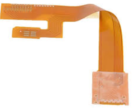
Advanced Techniques for Minimizing Crosstalk in PCB Design
In the realm of advanced printed circuit board (PCB) design, minimizing crosstalk is a critical consideration, particularly in high-speed layouts where signal integrity is paramount. Crosstalk, the unwanted coupling of signals between adjacent traces, can lead to data corruption, increased error rates, and overall system instability. As electronic devices become more compact and operate at higher frequencies, the challenge of mitigating crosstalk becomes increasingly significant. Therefore, understanding and implementing advanced techniques to minimize crosstalk is essential for engineers striving to maintain the performance and reliability of their designs.
One of the primary strategies for reducing crosstalk in PCB design is the careful management of trace spacing.
By increasing the distance between adjacent traces, the potential for electromagnetic interference is significantly reduced. This approach, however, must be balanced with the constraints of board size and component density. In high-speed layouts, where space is often at a premium, designers must judiciously allocate space to ensure adequate separation without compromising the overall design.
In addition to trace spacing, the use of ground planes is another effective method for minimizing crosstalk.
Ground planes act as a shield, absorbing and redirecting electromagnetic interference away from sensitive signal traces. By strategically placing ground planes adjacent to signal layers, designers can create a controlled environment that mitigates the effects of crosstalk. Furthermore, the implementation of ground vias, which connect the ground planes across multiple layers, enhances this shielding effect by providing a continuous path for interference to dissipate.
Moreover, differential signaling is a technique that can be employed to combat crosstalk in high-speed PCB layouts.
By transmitting signals as complementary pairs, differential signaling inherently cancels out noise and interference, as any external disturbance affects both lines equally and is thus negated. This method is particularly advantageous in environments with high levels of electromagnetic interference, as it enhances signal integrity and reduces susceptibility to crosstalk.
Another advanced technique involves the careful routing of signal traces.
Designers should aim to route high-speed signals on internal layers sandwiched between ground planes, a configuration known as stripline routing. This approach not only minimizes crosstalk but also provides a controlled impedance environment, which is crucial for maintaining signal integrity at high frequencies. Additionally, avoiding sharp angles and maintaining consistent trace widths can further reduce the potential for crosstalk by ensuring uniform signal propagation.
Furthermore, the use of simulation tools is indispensable in the design process for predicting and mitigating crosstalk.
These tools allow designers to model the electromagnetic interactions between traces and assess the impact of various design choices on signal integrity. By simulating different scenarios, engineers can identify potential sources of crosstalk and make informed decisions to optimize their layouts before physical prototyping.
In conclusion, minimizing crosstalk in advanced PCB layouts requires a multifaceted approach that combines strategic trace spacing, effective use of ground planes, differential signaling, careful routing, and simulation tools. As electronic devices continue to evolve, the demand for high-speed, reliable PCB designs will only increase, making the mastery of these techniques more crucial than ever. By implementing these advanced strategies, designers can ensure that their high-speed layouts maintain optimal performance and signal integrity, ultimately leading to more robust and reliable electronic systems.
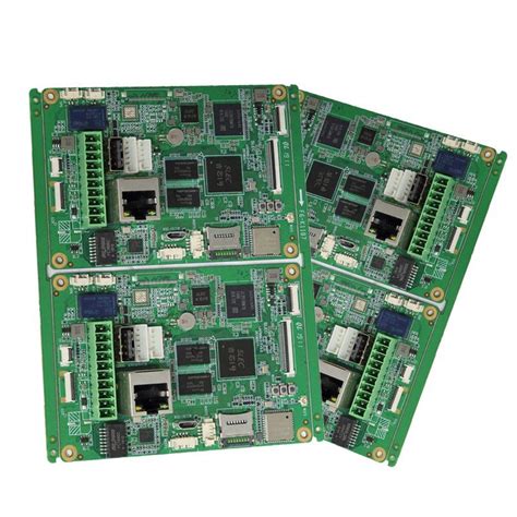
Power Distribution Network Design for High-Speed PCBs
In the realm of advanced printed circuit board (PCB) design, the power distribution network (PDN) plays a pivotal role, especially when dealing with high-speed layouts. As electronic devices continue to evolve, the demand for faster processing speeds and higher performance has necessitated the development of sophisticated PDN strategies. These strategies ensure that power is delivered efficiently and reliably to all components on the board, minimizing noise and maintaining signal integrity.
To begin with, the design of a PDN for high-speed PCBs requires a comprehensive understanding of the power requirements of each component.
This involves calculating the current demands and voltage levels necessary for optimal performance. By doing so, designers can create a power distribution scheme that meets these needs while also considering the constraints of the physical layout. Moreover, it is essential to account for the dynamic nature of power consumption, as components may have varying power needs depending on their operational states.
Transitioning to the layout considerations, one must pay close attention to the placement of power and ground planes.
These planes are crucial for providing a low-impedance path for current flow, which is vital for maintaining stable voltage levels across the board. In high-speed designs, the proximity of power and ground planes can significantly impact the overall performance of the PDN. By minimizing the distance between these planes, designers can reduce inductance and improve the board’s ability to handle high-frequency signals.
Furthermore, the use of decoupling capacitors is another critical aspect of PDN design.
These capacitors serve to smooth out voltage fluctuations and provide a local reservoir of charge for components that experience sudden changes in current demand. Strategically placing decoupling capacitors close to the power pins of integrated circuits can help mitigate issues related to power integrity. Additionally, selecting capacitors with appropriate values and characteristics is essential to ensure they effectively filter out high-frequency noise.
As we delve deeper into the intricacies of PDN design, it becomes apparent that managing impedance is a key factor in achieving a robust power distribution network.
Impedance mismatches can lead to reflections and signal degradation, which are particularly problematic in high-speed applications. To address this, designers often employ techniques such as impedance matching and controlled impedance routing. These methods help maintain consistent impedance levels throughout the board, thereby enhancing signal integrity and reducing the risk of electromagnetic interference.
In addition to these technical considerations, thermal management is another crucial element of PDN design for high-speed PCBs.
As components operate at higher speeds, they tend to generate more heat, which can adversely affect performance and reliability. Implementing effective thermal management solutions, such as heat sinks and thermal vias, can help dissipate heat and maintain optimal operating temperatures.
In conclusion, designing a power distribution network for high-speed PCBs is a complex task that requires careful planning and execution. By understanding the power requirements of components, optimizing the placement of power and ground planes, utilizing decoupling capacitors effectively, managing impedance, and addressing thermal concerns, designers can create a PDN that supports the high-speed operation of modern electronic devices. As technology continues to advance, the importance of a well-designed PDN will only grow, underscoring its critical role in the success of high-speed PCB layouts.
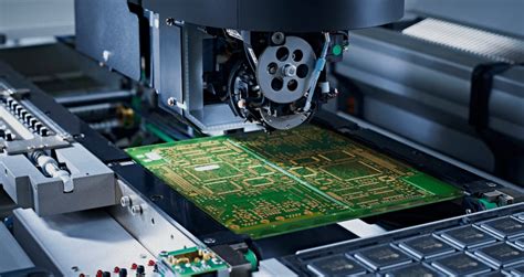
Implementing Differential Pair Routing in High-Speed PCB Layouts
In the realm of advanced printed circuit board (PCB) design, high-speed layouts have become increasingly critical due to the growing demand for faster and more efficient electronic devices. One of the essential techniques in high-speed PCB design is the implementation of differential pair routing. This method is pivotal in ensuring signal integrity and minimizing electromagnetic interference (EMI), which are crucial for the optimal performance of high-speed circuits. As we delve into the intricacies of differential pair routing, it is important to understand its fundamental principles and the benefits it offers in high-speed PCB layouts.
Differential pair routing involves the use of two complementary signals that are equal in magnitude but opposite in phase.
These signals travel along two parallel traces, known as a differential pair, which are designed to maintain a constant spacing and length throughout the PCB. This configuration helps to cancel out common-mode noise, as any external interference affects both traces equally and is subsequently negated at the receiving end. Consequently, differential pair routing significantly enhances signal integrity, making it indispensable in high-speed applications such as data communication and radio frequency (RF) circuits.
To implement differential pair routing effectively, designers must adhere to several key guidelines.
Firstly, maintaining equal trace lengths is paramount to ensure that the signals arrive simultaneously at the receiving end. Any discrepancy in length, known as skew, can lead to timing errors and degrade the performance of the circuit. To mitigate this, designers often employ serpentine routing techniques, which involve creating meanders in the traces to equalize their lengths. Additionally, maintaining a consistent spacing between the traces is crucial to preserve the characteristic impedance of the differential pair. This consistency helps to minimize reflections and signal loss, further enhancing the performance of the high-speed circuit.
Moreover, the choice of materials and layer stack-up in the PCB design plays a significant role in the effectiveness of differential pair routing.
High-frequency laminates with low dielectric constants are often preferred, as they reduce signal attenuation and dispersion. The layer stack-up should be designed to provide a controlled impedance environment, which is essential for maintaining signal integrity in high-speed applications. By carefully selecting materials and designing the layer stack-up, designers can optimize the performance of differential pairs and ensure reliable operation of the high-speed circuit.
In addition to these design considerations, the use of advanced simulation tools is invaluable in the implementation of differential pair routing.
These tools allow designers to model and analyze the behavior of differential pairs under various conditions, enabling them to identify potential issues and optimize the design before fabrication. By leveraging simulation tools, designers can achieve a higher level of precision and confidence in their high-speed PCB layouts.
In conclusion, the implementation of differential pair routing is a critical aspect of high-speed PCB design, offering significant advantages in terms of signal integrity and EMI reduction.
By adhering to best practices such as maintaining equal trace lengths, consistent spacing, and selecting appropriate materials, designers can effectively harness the benefits of differential pair routing. Furthermore, the use of advanced simulation tools enhances the design process, ensuring that high-speed circuits perform reliably and efficiently. As electronic devices continue to evolve, the importance of advanced PCB layout techniques, including differential pair routing, will only continue to grow, underscoring their vital role in the future of high-speed electronics.Optimizing Signal Integrity in High-Speed PCB Layouts
In the realm of modern electronics, the demand for faster and more efficient devices has led to the evolution of high-speed printed circuit board (PCB) layouts.
As the complexity of electronic systems increases, optimizing signal integrity becomes a critical aspect of PCB design. High-speed layouts, characterized by rapid signal transitions and high data rates, present unique challenges that require meticulous attention to detail. To ensure optimal performance, designers must consider various factors that influence signal integrity, including impedance control, crosstalk, and electromagnetic interference (EMI).
One of the fundamental aspects of optimizing signal integrity in high-speed PCB layouts is impedance control.
Impedance mismatches can lead to signal reflections, which degrade signal quality and can cause data errors. To mitigate this, designers must carefully select the appropriate trace widths and spacing, taking into account the dielectric properties of the substrate material. Additionally, the use of controlled impedance traces, such as microstrip or stripline configurations, can help maintain consistent impedance throughout the signal path. By ensuring that the impedance is matched across the entire circuit, signal reflections are minimized, thereby enhancing signal integrity.
In addition to impedance control, managing crosstalk is crucial in high-speed PCB layouts.
Crosstalk occurs when signals on adjacent traces interfere with each other, leading to unwanted noise and potential data corruption. To reduce crosstalk, designers can employ techniques such as increasing the spacing between traces, using ground planes to provide isolation, and routing critical signals on different layers. Furthermore, differential signaling, which involves using pairs of traces to carry signals, can be an effective strategy to minimize crosstalk. By utilizing these methods, designers can ensure that signals remain clean and free from interference, thus preserving signal integrity.
Electromagnetic interference (EMI) is another significant concern in high-speed PCB layouts.
EMI can originate from both internal and external sources, and it can adversely affect the performance of electronic systems. To combat EMI, designers can implement shielding techniques, such as using ground planes and metal enclosures, to contain and isolate electromagnetic fields. Additionally, careful component placement and routing can help minimize EMI by reducing loop areas and avoiding unnecessary coupling between traces. By addressing EMI concerns, designers can enhance the overall reliability and performance of high-speed PCBs.
Moreover, power integrity is an essential consideration in high-speed PCB layouts.
Fluctuations in power delivery can lead to voltage drops and noise, which can impact signal integrity. To ensure stable power delivery, designers can use decoupling capacitors strategically placed near power pins to filter out noise and provide a stable voltage supply. Additionally, employing a well-designed power distribution network (PDN) with low impedance paths can help maintain consistent power levels across the board. By optimizing power integrity, designers can support the high-speed operation of electronic components and maintain signal integrity.
In conclusion, optimizing signal integrity in high-speed PCB layouts is a multifaceted challenge that requires a comprehensive approach. By focusing on impedance control, crosstalk reduction, EMI mitigation, and power integrity, designers can create high-speed PCBs that deliver reliable and efficient performance. As technology continues to advance, the importance of signal integrity in high-speed designs will only grow, making it imperative for designers to stay informed about the latest techniques and best practices in PCB layout. Through careful planning and execution, high-speed PCB layouts can meet the demands of modern electronic systems, ensuring their success in an increasingly fast-paced world.

Advanced Techniques for Minimizing Crosstalk in PCB Design
In the realm of advanced printed circuit board (PCB) design, minimizing crosstalk is a critical consideration, particularly in high-speed layouts where signal integrity is paramount. Crosstalk, the unwanted coupling of signals between adjacent traces, can lead to data corruption, increased error rates, and overall system instability. As electronic devices become more compact and operate at higher frequencies, the challenge of mitigating crosstalk becomes increasingly significant. Therefore, understanding and implementing advanced techniques to minimize crosstalk is essential for engineers striving to maintain the performance and reliability of their designs.
One of the primary strategies for reducing crosstalk in PCB design is the careful management of trace spacing.
By increasing the distance between adjacent traces, the potential for electromagnetic interference is significantly reduced. This approach, however, must be balanced with the constraints of board size and component density. In high-speed layouts, where space is often at a premium, designers must judiciously allocate space to ensure adequate separation without compromising the overall design.
In addition to trace spacing, the use of ground planes is another effective method for minimizing crosstalk.
Ground planes act as a shield, absorbing and redirecting electromagnetic interference away from sensitive signal traces. By strategically placing ground planes adjacent to signal layers, designers can create a controlled environment that mitigates the effects of crosstalk. Furthermore, the implementation of ground vias, which connect the ground planes across multiple layers, enhances this shielding effect by providing a continuous path for interference to dissipate.
Moreover, differential signaling is a technique that can be employed to combat crosstalk in high-speed PCB layouts.
By transmitting signals as complementary pairs, differential signaling inherently cancels out noise and interference, as any external disturbance affects both lines equally and is thus negated. This method is particularly advantageous in environments with high levels of electromagnetic interference, as it enhances signal integrity and reduces susceptibility to crosstalk.
Another advanced technique involves the careful routing of signal traces.
Designers should aim to route high-speed signals on internal layers sandwiched between ground planes, a configuration known as stripline routing. This approach not only minimizes crosstalk but also provides a controlled impedance environment, which is crucial for maintaining signal integrity at high frequencies. Additionally, avoiding sharp angles and maintaining consistent trace widths can further reduce the potential for crosstalk by ensuring uniform signal propagation.
Furthermore, the use of simulation tools is indispensable in the design process for predicting and mitigating crosstalk..
These tools allow designers to model the electromagnetic interactions between traces and assess the impact of various design choices on signal integrity. By simulating different scenarios, engineers can identify potential sources of crosstalk and make informed decisions to optimize their layouts before physical prototyping.
In conclusion, minimizing crosstalk in advanced PCB layouts requires a multifaceted approach that combines strategic trace spacing, effective use of ground planes, differential signaling, careful routing, and simulation tools. As electronic devices continue to evolve, the demand for high-speed, reliable PCB designs will only increase, making the mastery of these techniques more crucial than ever. By implementing these advanced strategies, designers can ensure that their high-speed layouts maintain optimal performance and signal integrity, ultimately leading to more robust and reliable electronic systems.
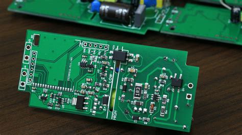
Power Distribution Network Design for High-Speed PCBs
In the realm of advanced printed circuit board (PCB) design, the power distribution network (PDN) plays a pivotal role, especially when dealing with high-speed layouts. As electronic devices continue to evolve, the demand for faster processing speeds and higher performance has necessitated the development of sophisticated PDN strategies. These strategies ensure that power is delivered efficiently and reliably to all components on the board, minimizing noise and maintaining signal integrity.
To begin with, the design of a PDN for high-speed PCBs requires a comprehensive understanding of the power requirements of each component.
This involves calculating the current demands and voltage levels necessary for optimal performance. By doing so, designers can create a power distribution scheme that meets these needs while also considering the constraints of the physical layout. Moreover, it is essential to account for the dynamic nature of power consumption, as components may have varying power needs depending on their operational states.
Transitioning to the layout considerations, one must pay close attention to the placement of power and ground planes.
These planes are crucial for providing a low-impedance path for current flow, which is vital for maintaining stable voltage levels across the board. In high-speed designs, the proximity of power and ground planes can significantly impact the overall performance of the PDN. By minimizing the distance between these planes, designers can reduce inductance and improve the board’s ability to handle high-frequency signals.
Furthermore, the use of decoupling capacitors is another critical aspect of PDN design.
These capacitors serve to smooth out voltage fluctuations and provide a local reservoir of charge for components that experience sudden changes in current demand. Strategically placing decoupling capacitors close to the power pins of integrated circuits can help mitigate issues related to power integrity. Additionally, selecting capacitors with appropriate values and characteristics is essential to ensure they effectively filter out high-frequency noise.
As we delve deeper into the intricacies of PDN design, it becomes apparent that managing impedance is a key factor in achieving a robust power distribution network.
Impedance mismatches can lead to reflections and signal degradation, which are particularly problematic in high-speed applications. To address this, designers often employ techniques such as impedance matching and controlled impedance routing. These methods help maintain consistent impedance levels throughout the board, thereby enhancing signal integrity and reducing the risk of electromagnetic interference.
In addition to these technical considerations, thermal management is another crucial element of PDN design for high-speed PCBs.
As components operate at higher speeds, they tend to generate more heat, which can adversely affect performance and reliability. Implementing effective thermal management solutions, such as heat sinks and thermal vias, can help dissipate heat and maintain optimal operating temperatures.
In conclusion, designing a power distribution network for high-speed PCBs is a complex task that requires careful planning and execution. By understanding the power requirements of components, optimizing the placement of power and ground planes, utilizing decoupling capacitors effectively, managing impedance, and addressing thermal concerns, designers can create a PDN that supports the high-speed operation of modern electronic devices. As technology continues to advance, the importance of a well-designed PDN will only grow, underscoring its critical role in the success of high-speed PCB layouts.
Implementing Differential Pair Routing in High-Speed PCB Layouts
In the realm of advanced printed circuit board (PCB) design, high-speed layouts have become increasingly critical due to the growing demand for faster and more efficient electronic devices. One of the essential techniques in high-speed PCB design is the implementation of differential pair routing. This method is pivotal in ensuring signal integrity and minimizing electromagnetic interference (EMI), which are crucial for the optimal performance of high-speed circuits. As we delve into the intricacies of differential pair routing, it is important to understand its fundamental principles and the benefits it offers in high-speed PCB layouts.
Differential pair routing involves the use of two complementary signals that are equal in magnitude but opposite in phase.
These signals travel along two parallel traces, known as a differential pair, which are designed to maintain a constant spacing and length throughout the PCB. This configuration helps to cancel out common-mode noise, as any external interference affects both traces equally and is subsequently negated at the receiving end. Consequently, differential pair routing significantly enhances signal integrity, making it indispensable in high-speed applications such as data communication and radio frequency (RF) circuits.
To implement differential pair routing effectively, designers must adhere to several key guidelines.
Firstly, maintaining equal trace lengths is paramount to ensure that the signals arrive simultaneously at the receiving end. Any discrepancy in length, known as skew, can lead to timing errors and degrade the performance of the circuit. To mitigate this, designers often employ serpentine routing techniques, which involve creating meanders in the traces to equalize their lengths. Additionally, maintaining a consistent spacing between the traces is crucial to preserve the characteristic impedance of the differential pair. This consistency helps to minimize reflections and signal loss, further enhancing the performance of the high-speed circuit.
Moreover, the choice of materials and layer stack-up in the PCB design plays a significant role in the effectiveness of differential pair routing.
High-frequency laminates with low dielectric constants are often preferred, as they reduce signal attenuation and dispersion. The layer stack-up should be designed to provide a controlled impedance environment, which is essential for maintaining signal integrity in high-speed applications. By carefully selecting materials and designing the layer stack-up, designers can optimize the performance of differential pairs and ensure reliable operation of the high-speed circuit.
In addition to these design considerations, the use of advanced simulation tools is invaluable in the implementation of differential pair routing.
These tools allow designers to model and analyze the behavior of differential pairs under various conditions, enabling them to identify potential issues and optimize the design before fabrication. By leveraging simulation tools, designers can achieve a higher level of precision and confidence in their high-speed PCB layouts.
In conclusion, the implementation of differential pair routing is a critical aspect of high-speed PCB design, offering significant advantages in terms of signal integrity and EMI reduction. By adhering to best practices such as maintaining equal trace lengths, consistent spacing, and selecting appropriate materials, designers can effectively harness the benefits of differential pair routing. Furthermore, the use of advanced simulation tools enhances the design process, ensuring that high-speed circuits perform reliably and efficiently. As electronic devices continue to evolve, the importance of advanced PCB layout techniques, including differential pair routing, will only continue to grow, underscoring their vital role in the future of high-speed electronics.Optimizing Signal Integrity in High-Speed PCB Layouts
In the realm of modern electronics, the demand for faster and more efficient devices has led to the evolution of high-speed printed circuit board (PCB) layouts.
As the complexity of electronic systems increases, optimizing signal integrity becomes a critical aspect of PCB design. High-speed layouts, characterized by rapid signal transitions and high data rates, present unique challenges that require meticulous attention to detail. To ensure optimal performance, designers must consider various factors that influence signal integrity, including impedance control, crosstalk, and electromagnetic interference (EMI).
One of the fundamental aspects of optimizing signal integrity in high-speed PCB layouts is impedance control.
Impedance mismatches can lead to signal reflections, which degrade signal quality and can cause data errors. To mitigate this, designers must carefully select the appropriate trace widths and spacing, taking into account the dielectric properties of the substrate material. Additionally, the use of controlled impedance traces, such as microstrip or stripline configurations, can help maintain consistent impedance throughout the signal path. By ensuring that the impedance is matched across the entire circuit, signal reflections are minimized, thereby enhancing signal integrity.
In addition to impedance control, managing crosstalk is crucial in high-speed PCB layouts.
Crosstalk occurs when signals on adjacent traces interfere with each other, leading to unwanted noise and potential data corruption. To reduce crosstalk, designers can employ techniques such as increasing the spacing between traces, using ground planes to provide isolation, and routing critical signals on different layers. Furthermore, differential signaling, which involves using pairs of traces to carry signals, can be an effective strategy to minimize crosstalk. By utilizing these methods, designers can ensure that signals remain clean and free from interference, thus preserving signal integrity.
Electromagnetic interference (EMI) is another significant concern in high-speed PCB layouts.
EMI can originate from both internal and external sources, and it can adversely affect the performance of electronic systems. To combat EMI, designers can implement shielding techniques, such as using ground planes and metal enclosures, to contain and isolate electromagnetic fields. Additionally, careful component placement and routing can help minimize EMI by reducing loop areas and avoiding unnecessary coupling between traces. By addressing EMI concerns, designers can enhance the overall reliability and performance of high-speed PCBs.
Moreover, power integrity is an essential consideration in high-speed PCB layouts.
Fluctuations in power delivery can lead to voltage drops and noise, which can impact signal integrity. To ensure stable power delivery, designers can use decoupling capacitors strategically placed near power pins to filter out noise and provide a stable voltage supply. Additionally, employing a well-designed power distribution network (PDN) with low impedance paths can help maintain consistent power levels across the board. By optimizing power integrity, designers can support the high-speed operation of electronic components and maintain signal integrity.
In conclusion, optimizing signal integrity in high-speed PCB layouts is a multifaceted challenge that requires a comprehensive approach. By focusing on impedance control, crosstalk reduction, EMI mitigation, and power integrity, designers can create high-speed PCBs that deliver reliable and efficient performance. As technology continues to advance, the importance of signal integrity in high-speed designs will only grow, making it imperative for designers to stay informed about the latest techniques and best practices in PCB layout. Through careful planning and execution, high-speed PCB layouts can meet the demands of modern electronic systems, ensuring their success in an increasingly fast-paced world.
Advanced Techniques for Minimizing Crosstalk in PCB Design
In the realm of advanced printed circuit board (PCB) design, minimizing crosstalk is a critical consideration, particularly in high-speed layouts where signal integrity is paramount. Crosstalk, the unwanted coupling of signals between adjacent traces, can lead to data corruption, increased error rates, and overall system instability. As electronic devices become more compact and operate at higher frequencies, the challenge of mitigating crosstalk becomes increasingly significant. Therefore, understanding and implementing advanced techniques to minimize crosstalk is essential for engineers striving to maintain the performance and reliability of their designs.
One of the primary strategies for reducing crosstalk in PCB design is the careful management of trace spacing.
By increasing the distance between adjacent traces, the potential for electromagnetic interference is significantly reduced. This approach, however, must be balanced with the constraints of board size and component density. In high-speed layouts, where space is often at a premium, designers must judiciously allocate space to ensure adequate separation without compromising the overall design.
In addition to trace spacing, the use of ground planes is another effective method for minimizing crosstalk.
Ground planes act as a shield, absorbing and redirecting electromagnetic interference away from sensitive signal traces. By strategically placing ground planes adjacent to signal layers, designers can create a controlled environment that mitigates the effects of crosstalk. Furthermore, the implementation of ground vias, which connect the ground planes across multiple layers, enhances this shielding effect by providing a continuous path for interference to dissipate.
Moreover, differential signaling is a technique that can be employed to combat crosstalk in high-speed PCB layouts.
By transmitting signals as complementary pairs, differential signaling inherently cancels out noise and interference, as any external disturbance affects both lines equally and is thus negated. This method is particularly advantageous in environments with high levels of electromagnetic interference, as it enhances signal integrity and reduces susceptibility to crosstalk.
Another advanced technique involves the careful routing of signal traces.
Designers should aim to route high-speed signals on internal layers sandwiched between ground planes, a configuration known as stripline routing. This approach not only minimizes crosstalk but also provides a controlled impedance environment, which is crucial for maintaining signal integrity at high frequencies. Additionally, avoiding sharp angles and maintaining consistent trace widths can further reduce the potential for crosstalk by ensuring uniform signal propagation.
Furthermore, the use of simulation tools is indispensable in the design process for predicting and mitigating crosstalk.
These tools allow designers to model the electromagnetic interactions between traces and assess the impact of various design choices on signal integrity. By simulating different scenarios, engineers can identify potential sources of crosstalk and make informed decisions to optimize their layouts before physical prototyping.
In conclusion, minimizing crosstalk in advanced PCB layouts requires a multifaceted approach that combines strategic trace spacing, effective use of ground planes, differential signaling, careful routing, and simulation tools. As electronic devices continue to evolve, the demand for high-speed, reliable PCB designs will only increase, making the mastery of these techniques more crucial than ever. By implementing these advanced strategies, designers can ensure that their high-speed layouts maintain optimal performance and signal integrity, ultimately leading to more robust and reliable electronic systems.

Power Distribution Network Design for High-Speed PCBs
In the realm of advanced printed circuit board (PCB) design, the power distribution network (PDN) plays a pivotal role, especially when dealing with high-speed layouts. As electronic devices continue to evolve, the demand for faster processing speeds and higher performance has necessitated the development of sophisticated PDN strategies. These strategies ensure that power is delivered efficiently and reliably to all components on the board, minimizing noise and maintaining signal integrity.
To begin with, the design of a PDN for high-speed PCBs requires a comprehensive understanding of the power requirements of each component.
This involves calculating the current demands and voltage levels necessary for optimal performance. By doing so, designers can create a power distribution scheme that meets these needs while also considering the constraints of the physical layout. Moreover, it is essential to account for the dynamic nature of power consumption, as components may have varying power needs depending on their operational states.
Transitioning to the layout considerations, one must pay close attention to the placement of power and ground planes.
These planes are crucial for providing a low-impedance path for current flow, which is vital for maintaining stable voltage levels across the board. In high-speed designs, the proximity of power and ground planes can significantly impact the overall performance of the PDN. By minimizing the distance between these planes, designers can reduce inductance and improve the board’s ability to handle high-frequency signals.
Furthermore, the use of decoupling capacitors is another critical aspect of PDN design.
These capacitors serve to smooth out voltage fluctuations and provide a local reservoir of charge for components that experience sudden changes in current demand. Strategically placing decoupling capacitors close to the power pins of integrated circuits can help mitigate issues related to power integrity. Additionally, selecting capacitors with appropriate values and characteristics is essential to ensure they effectively filter out high-frequency noise.
As we delve deeper into the intricacies of PDN design, it becomes apparent that managing impedance is a key factor in achieving a robust power distribution network.
Impedance mismatches can lead to reflections and signal degradation, which are particularly problematic in high-speed applications. To address this, designers often employ techniques such as impedance matching and controlled impedance routing. These methods help maintain consistent impedance levels throughout the board, thereby enhancing signal integrity and reducing the risk of electromagnetic interference.
In addition to these technical considerations, thermal management is another crucial element of PDN design for high-speed PCBs.
As components operate at higher speeds, they tend to generate more heat, which can adversely affect performance and reliability. Implementing effective thermal management solutions, such as heat sinks and thermal vias, can help dissipate heat and maintain optimal operating temperatures.
In conclusion, designing a power distribution network for high-speed PCBs is a complex task that requires careful planning and execution. By understanding the power requirements of components, optimizing the placement of power and ground planes, utilizing decoupling capacitors effectively, managing impedance, and addressing thermal concerns, designers can create a PDN that supports the high-speed operation of modern electronic devices. As technology continues to advance, the importance of a well-designed PDN will only grow, underscoring its critical role in the success of high-speed PCB layouts.
Implementing Differential Pair Routing in High-Speed PCB Layouts
In the realm of advanced printed circuit board (PCB) design, high-speed layouts have become increasingly critical due to the growing demand for faster and more efficient electronic devices.
One of the essential techniques in high-speed PCB design is the implementation of differential pair routing.
This method is pivotal in ensuring signal integrity and minimizing electromagnetic interference (EMI), which are crucial for the optimal performance of high-speed circuits. As we delve into the intricacies of differential pair routing, it is important to understand its fundamental principles and the benefits it offers in high-speed PCB layouts.
Differential pair routing involves the use of two complementary signals that are equal in magnitude but opposite in phase.
These signals travel along two parallel traces, known as a differential pair, which are designed to maintain a constant spacing and length throughout the PCB. This configuration helps to cancel out common-mode noise, as any external interference affects both traces equally and is subsequently negated at the receiving end. Consequently, differential pair routing significantly enhances signal integrity, making it indispensable in high-speed applications such as data communication and radio frequency (RF) circuits.
To implement differential pair routing effectively, designers must adhere to several key guidelines.
Firstly, maintaining equal trace lengths is paramount to ensure that the signals arrive simultaneously at the receiving end. Any discrepancy in length, known as skew, can lead to timing errors and degrade the performance of the circuit. To mitigate this, designers often employ serpentine routing techniques, which involve creating meanders in the traces to equalize their lengths. Additionally, maintaining a consistent spacing between the traces is crucial to preserve the characteristic impedance of the differential pair. This consistency helps to minimize reflections and signal loss, further enhancing the performance of the high-speed circuit.
Moreover, the choice of materials and layer stack-up in the PCB design plays a significant role in the effectiveness of differential pair routing.
High-frequency laminates with low dielectric constants are often preferred, as they reduce signal attenuation and dispersion. The layer stack-up should be designed to provide a controlled impedance environment, which is essential for maintaining signal integrity in high-speed applications. By carefully selecting materials and designing the layer stack-up, designers can optimize the performance of differential pairs and ensure reliable operation of the high-speed circuit.
In addition to these design considerations, the use of advanced simulation tools is invaluable in the implementation of differential pair routing.
These tools allow designers to model and analyze the behavior of differential pairs under various conditions, enabling them to identify potential issues and optimize the design before fabrication. By leveraging simulation tools, designers can achieve a higher level of precision and confidence in their high-speed PCB layouts.
In conclusion, the implementation of differential pair routing is a critical aspect of high-speed PCB design, offering significant advantages in terms of signal integrity and EMI reduction. By adhering to best practices such as maintaining equal trace lengths, consistent spacing, and selecting appropriate materials, designers can effectively harness the benefits of differential pair routing. Furthermore, the use of advanced simulation tools enhances the design process, ensuring that high-speed circuits perform reliably and efficiently. As electronic devices continue to evolve, the importance of advanced PCB layout techniques, including differential pair routing, will only continue to grow, underscoring their vital role in the future of high-speed electronics.

