Advanced PCB Manufacturing Tech Powering Next-Gen Devices

Key Takeaways
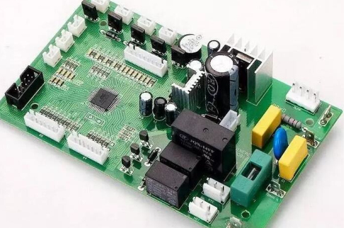
When exploring modern PCB manufacturing, you’ll find that advancements are reshaping how devices are designed and produced. PCB manufacturing companies now prioritize high-density interconnect (HDI) technology to meet the demand for smaller, faster electronics. By layering circuits vertically, HDI allows for miniaturization without sacrificing performance—critical for wearables and compact IoT devices.
“Optimizing PCB manufacturing cost requires balancing material innovation with process efficiency. Consider flexible substrates or additive techniques to reduce waste and improve yield.”
The rise of AI-driven processes is another game-changer. Automated defect detection and predictive maintenance streamline production, enabling PCB manufacturing businesses to deliver higher-quality boards at scale. For smart devices, this means faster time-to-market and enhanced reliability. Meanwhile, 5G connectivity demands boards with ultra-low latency and thermal stability, pushing companies to adopt advanced materials like high-frequency laminates.
Flexible circuits are unlocking new possibilities, especially for wearables. These bendable PCBs conform to unconventional shapes, making them ideal for health monitors and foldable displays. However, integrating these designs into existing workflows can challenge traditional PCB manufacturing practices, requiring tighter collaboration between designers and fabricators.
Sustainability is no longer optional. Leading PCB manufacturing companies are adopting recyclable substrates and halogen-free materials, reducing environmental impact without compromising durability. This shift not only aligns with global regulations but also appeals to eco-conscious consumers.
When planning your PCB manufacturing business, prioritize scalability. Techniques like additive manufacturing (3D-printed circuits) allow rapid prototyping, while modular production lines adapt to fluctuating demands. By leveraging these innovations, you can stay competitive in a market where IoT integration and miniaturization define success.
HDI Technology Redefining PCB Miniaturization
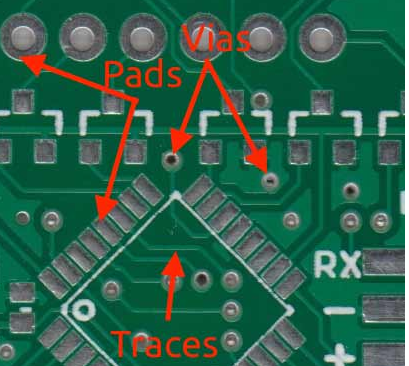
As device footprints shrink and performance demands escalate, PCB manufacturing faces a critical challenge: packing more functionality into tighter spaces. This is where High-Density Interconnect (HDI) technology emerges as a game-changer. By leveraging microvias, stacked copper layers, and ultra-fine line traces, HDI allows PCB manufacturing companies to create boards with up to 20% higher component density compared to traditional methods. For context, modern wearables and medical implants now integrate 12+ layers in designs thinner than 1.2mm – a feat unachievable with conventional processes.
The shift to HDI isn’t just about size reduction. It directly impacts PCB manufacturing cost by minimizing material waste through laser-drilled vias and optimizing layer counts. However, the initial investment in precision equipment can be substantial, pushing smaller PCB manufacturing businesses to partner with specialized fabricators. For example, industry leaders like Andwin PCB offer HDI prototyping services that reduce iteration cycles by 40%, making advanced designs accessible even for startups.
| Feature | Traditional PCB | HDI PCB |
|---|---|---|
| Minimum Trace Width | 100 µm | 50 µm |
| Via Diameter | 300 µm | 75 µm (laser-drilled) |
| Layer Count Range | 4-16 | 8-24+ |
| Typical Applications | Consumer Electronics | 5G Modules, Neural Implants |
What makes HDI indispensable for next-gen devices? First, signal integrity improves as shorter conductive paths reduce latency – crucial for 5G antennas and AI processors. Second, the ability to embed passive components within layers slashes assembly time while enhancing reliability. As you scale production, the per-unit PCB manufacturing cost drops significantly, offsetting upfront engineering expenses.
This evolution reshapes how PCB manufacturing companies approach R&D. Cross-disciplinary teams now collaborate early in the design phase to balance thermal management, impedance control, and manufacturability – a stark contrast to the linear workflows of the past. With IoT and edge computing pushing miniaturization limits further, HDI isn’t just an option; it’s the backbone of tomorrow’s compact electronics.
Flexible Circuits Enable Next-Gen Wearables
The rise of flexible circuits is transforming how you interact with wearable technology, enabling devices to conform seamlessly to your body while maintaining robust performance. Unlike traditional rigid boards, these bendable substrates leverage advanced materials like polyimide films and stretchable conductive inks, allowing PCB manufacturing companies to create ultra-thin, lightweight designs that withstand repeated bending and twisting. This innovation addresses a critical challenge in wearable PCB manufacturing: balancing durability with the need for compact, energy-efficient layouts.
By integrating high-density interconnects (HDI) into flexible designs, manufacturers achieve unprecedented circuit density without sacrificing reliability. This is particularly vital for health-monitoring wearables, where sensors must maintain consistent contact with skin while remaining unobtrusive. For instance, ECG patches and fitness trackers now embed multi-layer flexible PCBs that route signals through complex pathways—a feat impossible with conventional rigid boards.
The PCB manufacturing cost for flexible circuits has decreased significantly due to improved production techniques like roll-to-roll processing, making them viable for mass-market wearables. You’ll find these circuits in everything from smartwatches to medical patches, where their ability to conform to curved surfaces unlocks ergonomic designs. However, transitioning to flexible PCB production requires PCB manufacturing businesses to adopt new equipment and expertise, particularly in laser drilling and precision lamination.
As IoT and 5G drive demand for smaller, more adaptive electronics, flexible circuits are becoming a cornerstone of next-gen wearables. Their compatibility with additive manufacturing methods further accelerates prototyping cycles, letting engineers test form factors that merge seamlessly with textiles or biometric sensors. For brands aiming to lead in wearable tech, partnering with agile PCB manufacturing companies specializing in flexible solutions isn’t optional—it’s essential to staying ahead in a market where adaptability defines success.
AI-Driven PCB Manufacturing for Smart Devices
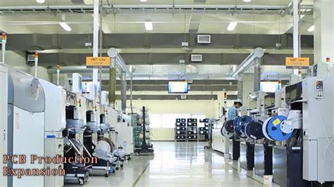
The integration of artificial intelligence into PCB manufacturing is transforming how smart devices are designed and produced. By leveraging machine learning algorithms, PCB manufacturing companies can now predict design flaws, optimize material usage, and automate complex processes that once required manual oversight. This shift not only accelerates production timelines but also reduces PCB manufacturing cost by minimizing waste and rework. For instance, AI-powered optical inspection systems detect microscopic defects in real time, ensuring higher yields for high-density interconnect (HDI) boards used in smartphones and IoT sensors.
As demand grows for smaller, more powerful electronics, AI-driven systems enable precise control over trace widths and layer alignment—critical factors in miniaturized designs. These technologies allow manufacturers to balance performance with scalability, a key consideration for businesses aiming to stay competitive in the PCB manufacturing business. Advanced analytics further refine supply chain decisions, predicting component shortages or price fluctuations that could impact production schedules.
What sets AI apart is its ability to learn from historical data. Over time, these systems identify patterns in design failures or material inefficiencies, offering actionable insights to engineers. For example, optimizing panel layouts to fit more circuits per board directly lowers PCB manufacturing cost while maintaining quality. This adaptability is particularly valuable for prototyping next-gen wearables or 5G modules, where rapid iteration cycles are essential.
However, implementing AI requires upfront investment in both hardware and workforce training. Leading PCB manufacturing companies address this by partnering with tech firms to develop customized solutions, ensuring seamless integration with existing workflows. The result? A smarter, more responsive production ecosystem that meets the evolving needs of compact, connected devices—without compromising on reliability or sustainability.
5G Connectivity Demands Advanced Circuit Designs
The rollout of 5G networks is pushing PCB manufacturing to evolve beyond traditional design limitations. With 5G’s higher frequencies and faster data rates, circuit boards must handle signal integrity challenges that older-generation designs never faced. PCB manufacturing companies now prioritize materials like low-loss laminates and advanced substrate technologies to minimize electromagnetic interference (EMI) and power dissipation. These innovations ensure that devices maintain seamless connectivity even in densely packed urban environments or high-interference industrial settings.
You’ll notice that PCB manufacturing cost considerations are shifting as well. While high-frequency materials like Rogers or Teflon-based substrates add upfront expenses, they reduce long-term losses from signal degradation—a critical trade-off for 5G-compatible devices. To stay competitive, PCB manufacturing businesses are adopting laser-drilled microvias and stacked via-in-pad designs, which improve routing density without compromising reliability. This is especially vital for applications like millimeter-wave antennas in smartphones or IoT gateways, where every square millimeter counts.
The integration of AI-driven simulation tools further streamlines design validation, allowing engineers to predict thermal performance and signal behavior before prototyping. Such advancements not only accelerate time-to-market but also lower iteration costs—a win-win for both manufacturers and end users. As 5G adoption grows, expect PCB manufacturing standards to increasingly emphasize impedance control tolerances and multilayer board alignment precision, ensuring networks deliver on their promise of ultra-low latency and gigabit-speed connectivity.

IoT Integration Reshapes PCB Production Standards
The proliferation of IoT devices—from smart sensors to connected appliances—is forcing PCB manufacturing companies to rethink traditional design and fabrication protocols. As billions of devices demand seamless connectivity, your PCB manufacturing business must now prioritize embedded antenna integration, multi-band signal integrity, and low-power consumption architectures. These requirements aren’t optional; they’re critical for meeting global certifications like IEEE 802.15.4 for IoT interoperability.
To keep PCB manufacturing costs competitive while scaling for IoT volumes, factories are adopting modular panelization techniques. By grouping multiple device-specific boards into single panels, you reduce material waste and streamline assembly—a necessity when producing PCBs for wearables or industrial sensors. Advanced laser direct imaging (LDI) systems further optimize precision, enabling trace widths under 25µm to accommodate dense component layouts without sacrificing signal clarity.
But IoT’s impact goes beyond design. Real-time production analytics are becoming non-negotiable. Smart factories now embed sensors directly into PCB manufacturing lines, monitoring variables like copper plating uniformity or solder paste viscosity. This data-driven approach minimizes defects in high-frequency RF boards, which are prone to performance issues if impedance mismatches exceed ±5%.
The shift also demands tighter collaboration between OEMs and PCB manufacturing partners. For example, automotive IoT modules require boards that withstand -40°C to 125°C thermal cycling—a specification that influences material choices like polyimide substrates or halogen-free laminates. By aligning early in the design phase, you avoid costly redesigns and ensure compliance with evolving Industry 4.0 benchmarks.
While these changes elevate production standards, they also create opportunities. Companies mastering IoT-optimized PCB fabrication can command premium pricing, especially in markets like healthcare IoT, where reliability directly impacts safety. The key lies in balancing innovation with scalability—a challenge reshaping the competitive landscape of modern electronics manufacturing.
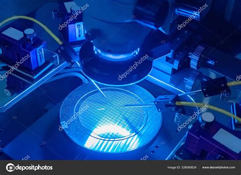
Additive Techniques Revolutionizing Board Fabrication
You’re witnessing a seismic shift in PCB manufacturing as additive techniques redefine how boards are built. Unlike traditional subtractive methods that etch away copper, additive manufacturing builds circuits layer by layer, slashing material waste by up to 70% while enabling precision unattainable with older processes. This approach isn’t just a novelty—it’s solving critical pain points for PCB manufacturing companies grappling with complex designs for 5G and IoT devices.
By leveraging technologies like 3D-printed conductive inks and aerosol jet deposition, manufacturers can now embed components directly into substrates, eliminating bulky connectors. This advancement directly addresses rising PCB manufacturing cost pressures, as additive processes reduce labor-intensive steps like drilling and plating. For instance, creating ultra-fine traces (under 15µm) becomes economically viable, a feat impractical with conventional methods.
The ripple effects extend to the PCB manufacturing business model itself. Companies adopting these techniques gain agility in prototyping—iterating designs in hours instead of weeks—while cutting raw material expenses. Imagine producing high-frequency RF circuits for aerospace applications with embedded antennas, all in a single print run. This capability is reshaping industries demanding lightweight, high-performance boards, from wearable health monitors to autonomous vehicle systems.
Critically, additive methods unlock design freedom for engineers. Multi-layer boards with irregular shapes or embedded sensors no longer require costly tooling changes. You’ll find this especially transformative for hybrid rigid-flex designs, where traditional fabrication struggles with alignment tolerances. The result? Faster time-to-market for compact, feature-rich devices without compromising reliability.
Yet challenges persist. Scaling additive production for mass volumes remains a hurdle, though advancements in multi-nozzle printing systems are bridging this gap. As the technology matures, expect tighter integration with AI-driven quality control systems—a natural progression for an industry prioritizing precision and sustainability. For now, forward-thinking PCB manufacturing companies are already redefining what’s possible, one printed layer at a time.
High-Density Interconnects Power Compact Electronics
As devices shrink but demand smarter functionality, PCB manufacturing pivots to high-density interconnect (HDI) technology to reconcile these competing needs. By packing more circuitry into smaller footprints through microvias, stacked layers, and finer trace widths, HDI allows wearables, medical implants, and 5G modules to maintain performance while shedding bulk. You’ll find this approach critical for applications where every millimeter matters—think foldable smartphones or IoT sensors embedded in industrial equipment.
For PCB manufacturing companies, adopting HDI isn’t just about keeping up with trends—it’s a strategic shift. Traditional fabrication methods struggle with the precision required for 8-12 layer boards featuring blind/buried vias. Laser drilling and advanced plating techniques become essential, which initially raises PCB manufacturing cost. However, the long-term payoff comes from reduced material waste and higher yields in mass production. Laser-direct imaging and automated optical inspection systems further streamline quality control, ensuring defects don’t derail complex designs.
This evolution also reshapes the PCB manufacturing business model. Clients now expect rapid prototyping cycles to test miniaturized designs, pushing manufacturers to balance speed with technical rigor. Meanwhile, thermal management grows trickier as components sit closer together. Solutions like embedded passive components and high-thermal-conductivity substrates mitigate overheating risks without compromising density.
While HDI’s complexity might seem daunting, its role in enabling next-gen electronics is non-negotiable. From aerospace avionics to consumer robotics, the drive for compactness hinges on how well PCB manufacturing innovates at the interconnect level. As device makers push boundaries, the industry’s ability to deliver reliable, high-density boards will separate leaders from laggards in the race for miniaturization.
Sustainable Materials in Modern PCB Innovations
As environmental regulations tighten and consumer demand for eco-conscious products grows, PCB manufacturing companies are pivoting toward sustainable material solutions without compromising performance. Traditional circuit boards often rely on non-recyclable substrates and hazardous chemicals, but innovations like halogen-free laminates and bio-based polymers are redefining production standards. These materials not only reduce environmental footprints but also align with global initiatives like RoHS and REACH, ensuring compliance while maintaining signal integrity in high-frequency applications.
The shift to sustainable practices impacts PCB manufacturing cost dynamics. While bio-compatible substrates may carry higher upfront expenses, they lower long-term liabilities by minimizing waste disposal fees and regulatory penalties. For instance, recyclable copper-clad laminates enable easier material recovery, cutting down on raw material consumption in the PCB manufacturing business. Additionally, water-based solder masks eliminate volatile organic compounds (VOCs), improving workplace safety and reducing ventilation system costs.
Forward-thinking manufacturers are also experimenting with mycelium-based packaging and chitosan coatings—materials derived from renewable sources—to replace plastic components. These alternatives not only degrade naturally but also maintain thermal stability critical for PCB manufacturing in high-temperature environments. By integrating these materials, companies can future-proof their supply chains against resource scarcity while appealing to eco-conscious clients in sectors like automotive and consumer electronics.
This transition isn’t just about compliance; it’s a strategic move to differentiate in competitive markets. As you evaluate partners for your next project, prioritize PCB manufacturing companies that balance innovation with sustainability—their material choices could define your product’s lifecycle efficiency and brand reputation.
Conclusion
The advancements driving modern PCB manufacturing underscore a pivotal shift in how devices are conceptualized and built. As you navigate this evolving landscape, understanding the synergy between miniaturization demands and production scalability becomes crucial. PCB manufacturing companies now leverage AI-driven processes not just to enhance precision but to dynamically optimize PCB manufacturing cost—a critical factor when balancing high-performance outputs with market competitiveness.
What sets apart today’s PCB manufacturing business models is their dual focus on innovation and adaptability. Flexible circuits, once niche, now enable wearables that conform to human motion, while additive techniques reduce material waste by up to 40%, aligning with both economic and sustainability goals. For industries like 5G and IoT, where signal integrity and space constraints dominate, high-density interconnects (HDIs) have transitioned from luxury to necessity.
Yet, success hinges on more than technical prowess. As you evaluate partners or strategies, consider how real-time analytics and modular production lines future-proof operations against shifting standards. The integration of eco-friendly substrates, for instance, isn’t just about compliance—it’s a strategic move to mitigate supply chain risks and appeal to environmentally conscious markets.
Ultimately, the trajectory of PCB manufacturing reflects a broader truth: tomorrow’s electronics won’t just be smaller or faster—they’ll demand architectures that seamlessly blend durability, efficiency, and intelligence. Whether you’re prototyping cutting-edge medical devices or scaling smart home systems, aligning with innovators who master this balance will define your competitive edge in the age of connected everything.
Frequently Asked Questions
How does HDI technology affect PCB manufacturing costs?
While high-density interconnect (HDI) techniques initially raise PCB manufacturing expenses due to specialized materials and precision requirements, they reduce long-term costs by enabling smaller, lighter boards. This optimization lowers material waste and supports miniaturization trends in wearables and IoT devices.
What makes PCB manufacturing companies adopt AI-driven processes?
Leading PCB manufacturing companies integrate AI-driven workflows to enhance yield rates and predict defects in real time. Machine learning algorithms analyze production data to refine etching tolerances and layer alignment, ensuring compliance with 5G and IoT design standards while maintaining competitive PCB manufacturing business margins.
Can flexible circuits reduce PCB manufacturing waste?
Yes, flexible PCB substrates like polyimide allow bendable designs that minimize material overuse. This adaptability supports irregular shapes in smart medical devices and foldable electronics, aligning with sustainability goals while addressing PCB manufacturing cost pressures through efficient resource utilization.
Why do advanced PCB manufacturing techniques prioritize additive processes?
Additive manufacturing reduces chemical usage by 40-60% compared to traditional subtractive methods. Techniques like inkjet printing enable precise conductive trace deposition, accelerating prototyping cycles for 5G antennas and high-frequency RF modules—critical for next-gen connectivity solutions.
How does IoT integration impact PCB manufacturing business models?
IoT-compatible designs demand embedded sensors and ultra-low-power components, pushing PCB manufacturing companies to adopt hybrid rigid-flex boards. This shift requires investments in laser-drilled microvias and thermal management layers, but opens revenue streams in smart infrastructure and industrial automation markets.
Ready to Optimize Your PCB Project?
For tailored solutions in PCB manufacturing that balance innovation and PCB manufacturing cost, please click here to explore advanced fabrication options for your next-gen devices.