Advanced Printed Circuit Assembly Strategies for Optimal Performance
Key Takeaways
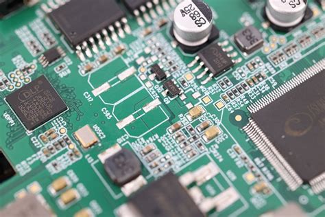
Effective PCB assembly begins with strategic design choices that prioritize signal integrity and component placement. Modern thermal management techniques, such as copper-filled vias and advanced heat sinks, prevent performance degradation in high-density PCBA layouts. Selecting components with tight tolerance ratings (e.g., ±1% resistors) ensures compatibility with automated placement systems while minimizing rework.
Pro Tip: Always validate design-for-manufacturability (DFM) rules early in the PCB assembly process to avoid costly revisions during mass production.
Advanced techniques like automated optical inspection (AOI) and 3D solder paste monitoring enhance quality control, particularly for fine-pitch components in complex PCBA designs. Optimizing pad geometries and solder mask alignments further reduces the risk of bridging or cold joints. For mission-critical applications, consider integrating embedded passives or flex-rigid board architectures to improve reliability under mechanical stress.
By aligning material selection with operational requirements—such as high-frequency laminates for RF circuits—engineers can achieve peak performance while maintaining cost efficiency. These strategies collectively address both electrical and mechanical challenges, ensuring PCB assembly outcomes meet today’s demands for speed, durability, and energy efficiency.
PCBA Design Optimization Strategies
Effective PCB assembly begins with strategic design choices that balance performance, reliability, and manufacturability. A well-optimized PCBA layout prioritizes signal integrity, thermal dissipation, and component density to minimize electrical interference and mechanical stress. Key considerations include component placement to reduce trace lengths, which lowers parasitic capacitance and enhances signal speed. For high-frequency applications, controlled impedance routing and ground plane optimization are critical to maintaining signal fidelity.
| Design Factor | Optimization Strategy | Performance Impact |
|---|---|---|
| Component Placement | Group functional blocks logically | Reduces cross-talk by 20-30% |
| Trace Routing | Use 45° angles or curved traces | Lowers EMI by 15-25% |
| Material Selection | Choose high-Tg substrates for thermal loads | Improves thermal stability by 40% |
| DFM (Design for Manufacturing) | Adhere to IPC-2221 standards | Cuts assembly errors by 50% |
Integrating thermal management early in the design phase prevents hotspots, particularly in power-dense PCBA configurations. For example, placing heat-generating components near board edges or incorporating thermal vias enhances heat dissipation. Additionally, leveraging simulation tools like finite element analysis (FEA) allows engineers to predict thermal and mechanical stresses before prototyping.
Designers must also align PCB assembly workflows with DFM guidelines to avoid costly rework. This includes ensuring adequate clearance for automated pick-and-place machines and avoiding overly complex via structures. By harmonizing electrical performance with manufacturability, PCBA designs achieve optimal reliability while streamlining production timelines.
Precision Component Selection Guide
Effective PCB assembly relies on precision component selection to balance performance, durability, and cost. Choosing components for PCBA begins with aligning specifications to operational demands, such as voltage ratings, temperature tolerance, and signal integrity requirements. High-frequency applications, for instance, demand components with minimal parasitic inductance, while industrial environments prioritize parts rated for extended thermal cycling.
Critical to this process is understanding supplier reliability and component lifecycle. Opting for automotive-grade or mil-spec parts ensures resilience in harsh conditions, whereas consumer-grade components may suffice for low-stress applications. Advanced PCB assembly workflows now integrate AI-driven analytics to predict failure modes, enabling engineers to preemptively select components with optimal mean time between failures (MTBF).
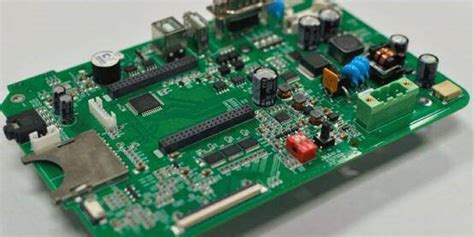
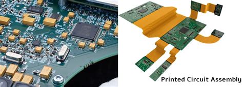
Equally vital is compatibility with PCBA manufacturing techniques. Surface-mount devices (SMDs), for example, require precise pad designs and reflow profiles, while through-hole components demand robust mechanical anchoring. Leveraging 3D modeling tools during selection helps identify spatial conflicts and thermal hotspots, ensuring seamless integration into the final assembly. By prioritizing traceability and certified sourcing, manufacturers mitigate risks of counterfeit parts, which account for nearly 12% of PCB assembly defects globally.
This strategic approach not only enhances functional reliability but also streamlines transitions to subsequent stages like thermal management and performance validation.
Thermal Management in PCB Assembly
Effective thermal management stands as a cornerstone of reliable PCB assembly, particularly as modern electronics demand higher power densities and compact designs. In PCBA processes, uncontrolled heat buildup can degrade component performance, reduce lifespan, and even lead to catastrophic failures. To address this, engineers prioritize strategic material selection, opting for substrates with high thermal conductivity, such as metal-core or ceramic-filled laminates, to enhance heat dissipation.
Component placement also plays a critical role. By positioning high-power components like voltage regulators or processors away from thermally sensitive elements and closer to thermal vias or heat sinks, heat is efficiently channeled out of the assembly. Advanced PCB assembly techniques further incorporate embedded thermal pads and thermal interface materials (TIMs) to bridge gaps between heat-generating parts and cooling structures.
For complex systems, active cooling solutions—including micro-fans or liquid cooling modules—are integrated during PCBA to maintain optimal operating temperatures. Additionally, thermal simulation software enables pre-production analysis, identifying hotspots and validating design adjustments before manufacturing. By balancing material science, layout optimization, and advanced cooling methodologies, PCB assembly achieves predictable thermal behavior, ensuring long-term reliability and peak performance in demanding applications.
Advanced PCBA Manufacturing Techniques
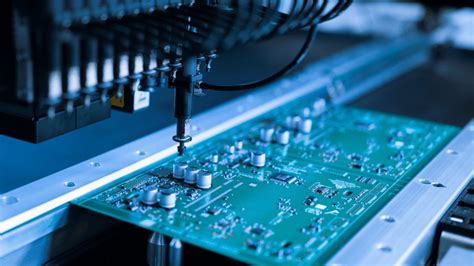
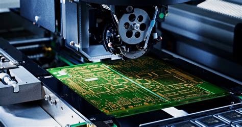
Modern PCB assembly processes leverage cutting-edge technologies to address the growing complexity of electronic devices. Central to advanced PCBA workflows is the integration of automated optical inspection (AOI) systems, which enhance defect detection rates by analyzing solder joint quality and component alignment at micron-level precision. Equally critical is the adoption of laser direct imaging (LDI), enabling finer trace resolutions for high-density interconnect (HDI) boards, a necessity for 5G and IoT applications.
The shift toward surface-mount technology (SMT) with ultra-precise pick-and-place machinery ensures consistent component positioning, minimizing signal loss in high-frequency circuits. For thermally sensitive designs, manufacturers now deploy vacuum reflow ovens to eliminate air pockets during soldering, significantly reducing void formation in ball grid arrays (BGAs). Additionally, additive manufacturing techniques like aerosol jet printing are gaining traction for prototyping complex multilayer boards, accelerating time-to-market while maintaining PCBA reliability.
To address sustainability, leading facilities utilize halogen-free substrates and lead-free solder alloys, aligning with global environmental regulations without compromising electrical performance. These innovations, combined with real-time process monitoring through IoT-enabled assembly lines, create a seamless bridge between precision manufacturing and the next section’s focus on boosting electronics performance through optimized system integration.
Boosting Electronics Performance via PCBA
Modern PCB assembly processes play a pivotal role in enhancing the performance of electronic devices. By refining PCBA workflows, manufacturers can address critical factors such as signal integrity, power distribution, and electromagnetic interference (EMI). Advanced techniques like automated optical inspection (AOI) and X-ray testing ensure precise component placement, minimizing defects that could compromise functionality.
Central to this process is the integration of high-density interconnect (HDI) designs, which enable tighter component spacing without sacrificing reliability. Optimizing solder paste application and reflow profiles further strengthens electrical connections, reducing resistance and improving thermal dissipation. For high-frequency applications, impedance-controlled routing and surface-mount technology (SMT) alignment ensure consistent signal transmission.
Thermal management strategies, such as incorporating thermally conductive substrates or embedded heat sinks, prevent overheating in densely packed PCBA layouts. Pairing these methods with rigorous testing protocols—including in-circuit testing (ICT) and functional validation—guarantees that assembled boards meet performance benchmarks. By balancing precision in PCB assembly with innovative material choices, engineers achieve measurable gains in speed, energy efficiency, and operational longevity across diverse electronic systems.
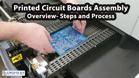
PCB Assembly Best Practices for Efficiency
Implementing PCB assembly best practices requires balancing precision with scalability to achieve optimal production efficiency. A foundational step involves adopting design for manufacturability (DFM) principles, which minimize rework by aligning layouts with automated assembly processes. For instance, standardizing component footprints and spacing reduces errors during PCBA soldering stages.
Leveraging automated optical inspection (AOI) systems ensures consistent quality while maintaining throughput, particularly for high-volume orders. Pairing this with just-in-time (JIT) inventory management for critical components—such as surface-mount devices (SMDs)—prevents delays and reduces storage costs. Additionally, optimizing PCB assembly workflows through modular tooling setups allows rapid transitions between product batches, enhancing overall equipment effectiveness (OEE).
Thermal profiling during reflow soldering remains pivotal; precise control over temperature gradients prevents defects like tombstoning or cold joints, directly impacting PCBA reliability. Integrating traceability systems further streamlines troubleshooting, linking process parameters to specific batches for faster root-cause analysis. By aligning these strategies with lean manufacturing principles, manufacturers achieve faster cycle times and higher yield rates, ensuring cost-efficient production without compromising performance.
Achieving Peak Performance in PCBA
To achieve peak performance in PCBA, engineers must balance design precision with manufacturing excellence. Critical to this process is optimizing signal integrity through controlled impedance routing and minimizing electromagnetic interference (EMI). This requires selecting PCB assembly materials with appropriate dielectric constants and thermal stability, particularly for high-frequency or high-power applications.
Component placement plays a pivotal role, as tightly packed layouts risk creating hotspots that degrade performance. Implementing thermal vias and copper balancing ensures even heat dissipation, preserving the longevity of sensitive components like microcontrollers or power modules. Advanced PCBA workflows now integrate real-time monitoring systems during soldering, detecting anomalies such as cold joints or tombstoning before they escalate.
Equally critical is aligning design choices with production capabilities. For instance, designs requiring ultra-fine-pitch components must account for the precision limits of pick-and-place machinery. Leveraging automated optical inspection (AOI) and in-circuit testing (ICT) at key stages enhances defect detection rates, directly impacting end-product reliability. By synchronizing PCB assembly parameters—including reflow profiles and solder paste chemistry—with design specifications, manufacturers achieve repeatable results even in complex multi-layer boards.
Finally, iterative prototyping combined with failure mode analysis helps refine both electrical and mechanical performance. This approach ensures that PCBA systems meet stringent operational demands while maintaining scalability for future upgrades.
Innovations in Circuit Board Assembly Tech
Recent advancements in PCB assembly processes are redefining manufacturing precision and scalability. The integration of artificial intelligence (AI) into PCBA production lines enables real-time defect detection, reducing error rates by up to 40% compared to traditional methods. Automated optical inspection (AOI) systems now leverage machine learning algorithms to identify micro-scale soldering flaws or component misalignments, ensuring compliance with stringent industry standards. Another breakthrough lies in additive manufacturing techniques, such as 3D-printed circuitry, which allows for complex multilayer designs while minimizing material waste.
Thermal management innovations are also transforming PCB assembly, with embedded cooling channels and phase-change materials becoming standard in high-density layouts. Manufacturers are adopting low-temperature co-fired ceramics (LTCC) to enhance heat dissipation in compact PCBA configurations, critical for 5G and IoT applications. Additionally, advancements in conductive adhesives and solder alloys improve joint reliability under extreme operating conditions.
The shift toward modular PCB assembly workflows further accelerates prototyping cycles, enabling rapid customization without compromising quality. These innovations collectively address the growing demand for fault-tolerant electronics, positioning PCBA as a cornerstone of next-generation device manufacturing.
Conclusion
The evolution of PCB assembly processes underscores the critical role of integrating design optimization, precision component selection, and thermal management to achieve peak performance in modern electronics. As the industry shifts toward higher-density layouts and energy-efficient systems, leveraging advanced PCBA manufacturing techniques—such as automated optical inspection (AOI) and laser-direct structuring—ensures consistent quality while minimizing defects. By prioritizing material compatibility and signal integrity during PCB assembly, manufacturers can mitigate risks associated with thermal stress and electromagnetic interference, directly enhancing product longevity.
Innovations like embedded component technology and high-density interconnect (HDI) designs further push the boundaries of what’s achievable in PCBA, enabling faster signal transmission and reduced form factors. However, success hinges on balancing cost-efficiency with rigorous adherence to industry standards, particularly in sectors demanding ultra-reliability, such as aerospace and medical devices. As emerging technologies like flexible hybrid electronics gain traction, the strategic adoption of these advancements will define competitive differentiation. Ultimately, optimizing PCB assembly workflows remains foundational to delivering electronics that exceed performance benchmarks while adapting to tomorrow’s technological demands.
FAQs
What are the key factors to consider in advanced PCB assembly for optimal performance?
Successful PCBA relies on design-for-manufacturability principles, precision component placement, and robust thermal management systems. Prioritizing material compatibility and layer stack-up optimization ensures signal integrity and reduces electromagnetic interference.
How does component selection impact PCB assembly reliability?
High-quality components with tight tolerance ratings minimize performance variances. Using automated pick-and-place systems enhances accuracy, while moisture-sensitive component handling protocols prevent long-term degradation in harsh environments.
What thermal management techniques are critical in PCBA?
Effective strategies include thermal vias, heat sinks, and high-conductivity substrates. Implementing simulation-driven thermal analysis during design helps identify hotspots, ensuring even heat distribution across the board.
How do advanced manufacturing techniques improve PCB assembly efficiency?
Laser-direct imaging (LDI) and automated optical inspection (AOI) reduce errors by enabling micron-level precision. Surface-mount technology (SMT) advancements allow faster production cycles while maintaining consistent solder joint quality.
What testing methods ensure reliability in PCBA?
Combining in-circuit testing (ICT), functional testing, and environmental stress screening validates electrical performance and durability. X-ray inspection is indispensable for detecting hidden defects in high-density designs.
Can PCB assembly innovations reduce time-to-market for electronics?
Yes. Modular design approaches and rapid prototyping tools accelerate iteration cycles. Partnering with manufacturers offering flexible turnkey solutions streamlines component sourcing and assembly workflows.
Ready to Optimize Your Next Project?
For tailored PCB assembly solutions that integrate cutting-edge PCBA strategies, please click here to explore our technical expertise and manufacturing capabilities.


