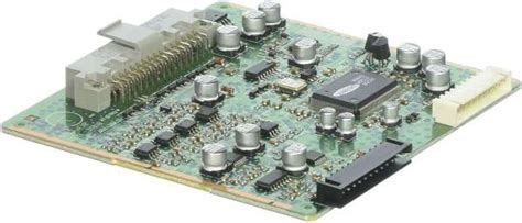
Advanced SMT PCB Assembly Equipment for High-Precision Manufacturing
Key Takeaways
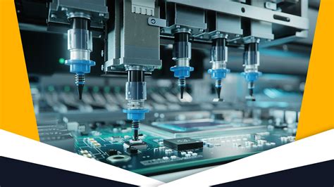
Modern PCB assembly processes leverage SMT equipment to achieve micron-level placement accuracy, with vision-guided placement systems now achieving ±15μm precision. These advancements enable PCBA manufacturers to handle components as small as 01005 (0.4 x 0.2 mm) while maintaining throughput exceeding 50,000 components per hour.
| Feature | Traditional Equipment | Advanced SMT Systems |
|---|---|---|
| Placement Accuracy | ±35μm | ±15μm |
| Component Size Support | 0402 (1.0 x 0.5 mm) | 01005 (0.4 x 0.2 mm) |
| Throughput (CPH) | 20,000–30,000 | 50,000–80,000 |
| Defect Detection Rate | 85–90% | 99.5%+ |
"The integration of real-time process monitoring in PCB assembly lines has reduced rework rates by 62% compared to manual inspection methods." – Industry Quality Report 2023
Three critical improvements define contemporary SMT PCB assembly equipment:
- Closed-loop feedback systems adjusting solder paste deposition during runtime
- Automated optical inspection (AOI) with machine learning-based defect classification
- Modular conveyor designs enabling rapid line reconfiguration
For manufacturers upgrading PCBA capabilities, prioritize equipment with:
- Multi-stage thermal profiling for lead-free soldering
- Compatible interfaces with existing MES/MOM platforms
- Predictive maintenance algorithms reducing downtime
Transitioning to next-gen systems requires evaluating return on precision – while advanced SMT equipment increases initial capital expenditure, it typically achieves ROI within 18 months through reduced scrap rates and improved first-pass yield.
Automation Innovations in SMT PCB Assembly
The integration of robotic placement systems and AI-driven process control has redefined efficiency in PCB assembly workflows. Modern PCBA production lines now leverage vision-guided pick-and-place machines capable of positioning components with ±15μm accuracy, paired with smart conveyor systems that dynamically adjust throughput based on real-time diagnostics. These systems minimize human intervention while maintaining micron-level precision, even when handling ultra-fine-pitch components below 0.3mm. Advanced machine learning algorithms further optimize solder paste deposition and reflow profiles, reducing defect rates by over 35% compared to traditional methods.
A critical advancement lies in closed-loop feedback mechanisms, where inline inspection tools instantly relay data to placement machines, enabling self-correction during PCB assembly. This seamless coordination between automated optical inspection (AOI) and component mounting systems ensures consistent quality without sacrificing speed. Manufacturers adopting these innovations report 20-50% faster cycle times while achieving six-sigma yield levels in high-density PCBA applications. As production scales, such automation not only addresses precision demands but also adapts effortlessly to evolving design complexities in consumer electronics, automotive systems, and IoT devices.
Precision Engineering in Modern PCB Manufacturing
Modern PCB assembly processes demand unparalleled precision to meet the evolving requirements of miniaturized electronics. Advanced SMT PCB assembly equipment now integrates laser-aligned placement systems and micro-meter-scale solder paste dispensers, ensuring components as small as 01005 packages are positioned with sub-micron accuracy. These innovations address critical challenges in PCBA, such as thermal management and signal integrity, by maintaining consistent solder joint geometry across high-density boards.
Automation plays a pivotal role, with vision-guided robotic arms and real-time feedback loops compensating for material variances and environmental fluctuations. For instance, adaptive conveyor systems adjust speed dynamically to optimize placement accuracy without sacrificing throughput. This synergy between hardware and software enables manufacturers to achieve zero-defect thresholds in sectors like medical devices and aerospace, where reliability is non-negotiable.
Furthermore, advancements in multi-stage inspection systems—combining 3D AOI (Automated Optical Inspection) and AI-powered defect detection—ensure every PCBA unit meets stringent quality benchmarks. As production demands evolve toward flexible, high-mix workflows, precision engineering remains the backbone of scalable, error-free manufacturing. By leveraging these technologies, manufacturers not only enhance product performance but also reduce rework costs, aligning with the industry’s shift toward sustainable, waste-minimized practices.
Boosting Throughput With SMT Assembly Tools
Modern PCB assembly workflows rely on SMT assembly tools to achieve unprecedented production speeds while maintaining strict quality benchmarks. Automated pick-and-place systems, equipped with high-precision vision alignment, now operate at rates exceeding 50,000 components per hour, reducing cycle times by up to 40% compared to conventional methods. These tools integrate seamlessly with PCBA lines, enabling synchronized workflows from solder paste application to final inspection.
Advanced feeders and nozzle technologies minimize component misalignment, while adaptive conveyor systems ensure continuous material flow, even for complex, multi-layer boards. Manufacturers leveraging modular SMT assembly equipment report throughput improvements of 25–35%, particularly when deploying dual-lane configurations for parallel processing. Real-time monitoring systems further optimize output by identifying bottlenecks in solder paste deposition or reflow stages, allowing instant adjustments without halting production.
The integration of PCBA-specific software suites enhances throughput by automating programming for diverse board designs, reducing setup times by over 60%. This agility is critical for high-mix production environments, where rapid changeovers between product variants are essential. By combining ultra-responsive motion control with predictive maintenance algorithms, next-gen SMT assembly tools not only accelerate output but also extend equipment lifespan, ensuring sustained productivity gains across electronics manufacturing ecosystems.
Smart Quality Control for Electronics Production
Modern PCB assembly processes demand unprecedented precision, driving the integration of intelligent inspection systems into PCBA production lines. Advanced vision systems equipped with high-resolution cameras and machine learning algorithms now perform automated optical inspection (AOI) at micron-level accuracy, identifying defects like solder bridging or component misalignment in real time. These systems analyze up to 10,000 data points per minute, correlating findings with historical quality metrics to refine detection thresholds dynamically.
To ensure consistency, inline testing modules are embedded within SMT assembly equipment, enabling immediate feedback loops that adjust placement pressure or reflow oven temperatures. For example, AI-driven predictive analytics can flag potential failures in BGA (ball grid array) soldering before boards advance to subsequent stages, reducing rework rates by up to 40%. Additionally, 3D X-ray inspection tools validate hidden connections in multilayer boards, critical for aerospace or medical-grade PCBA applications.
By merging IoT-enabled sensors with centralized quality management platforms, manufacturers achieve end-to-end traceability, linking every defect to specific machine parameters or material batches. This shift not only elevates yield rates but also aligns with Industry 4.0 standards, where smart quality control becomes a cornerstone of agile, data-driven electronics manufacturing.
Next-Gen SMT Equipment for Enhanced Accuracy
Modern PCB assembly processes demand unprecedented precision to meet the evolving requirements of compact, high-performance electronics. Next-generation SMT equipment integrates laser-aligned placement systems and adaptive vision technologies to achieve micron-level accuracy in component positioning. These systems leverage real-time feedback loops, correcting placement errors within milliseconds to ensure PCBA outcomes align with design specifications—even for components smaller than 0.4mm.
Advanced machines now incorporate 3D solder paste inspection (SPI) and AI-driven defect detection, which work synergistically to minimize soldering inconsistencies before reflow. This dual-layer verification reduces rework rates by up to 40%, directly enhancing manufacturing efficiency. Additionally, modular designs in newer SMT platforms allow rapid reconfiguration for mixed-product batches, maintaining precision across diverse PCB assembly workflows.
The integration of machine learning algorithms further refines calibration processes, automatically adjusting for environmental variables like humidity or thermal drift. Such innovations ensure consistent accuracy in PCBA production, even under dynamic operating conditions. By combining high-speed capabilities with sub-micron repeatability, next-gen SMT tools are redefining quality benchmarks for applications ranging from medical devices to aerospace electronics.
Optimizing PCB Assembly With Advanced Automation
Modern PCB assembly processes achieve unprecedented efficiency through intelligent automation systems that integrate robotic precision with real-time data analytics. Automated PCBA lines now deploy vision-guided robotic arms for component placement accuracy within ±25 microns, eliminating manual errors while maintaining high-speed throughput exceeding 80,000 components per hour. These systems leverage closed-loop feedback mechanisms, where machine learning algorithms continuously refine placement patterns based on thermal and vibration data from high-density interconnect (HDI) boards.
A critical advancement lies in automated optical inspection (AOI) modules embedded directly into production lines. These systems perform multi-spectral imaging at 3D angles, detecting solder joint defects as small as 15μm—a 60% improvement over legacy methods. For PCB assembly workflows handling mixed-technology boards, hybrid feeders automatically switch between surface-mount (SMD) and through-hole components without downtime, reducing changeover delays by 92%.
The synergy between PCBA automation and enterprise resource planning (ERP) software further optimizes material flow, with smart conveyors adjusting speeds dynamically based on downstream bottlenecks. This integration cuts work-in-progress inventory by 40% while ensuring traceability through blockchain-enabled tracking for compliance-driven industries. As manufacturers adopt these technologies, the balance between ultra-fine-pitch component handling and scalable production capacity redefines what’s achievable in precision electronics manufacturing.
High-Speed SMT Solutions for Precision Output
The demand for faster production cycles in PCB assembly has driven significant advancements in high-speed surface-mount technology (SMT) systems. Modern PCBA lines now integrate multi-functional gantry systems capable of mounting 80,000 components per hour while maintaining ±25μm accuracy. These solutions leverage adaptive vision systems to detect micro-scale defects in real time, ensuring consistent quality even at accelerated throughput rates.
A critical innovation lies in dynamic thermal profiling, which optimizes reflow soldering processes for diverse component types—from fine-pitch ICs to bulky connectors—without sacrificing speed. By synchronizing pick-and-place robots with AI-driven planning algorithms, manufacturers achieve zero-defect targets while reducing setup times by 40% in mixed-product environments. For industries like automotive electronics or medical devices, where PCB assembly tolerances are measured in microns, such precision ensures compliance with stringent reliability standards.
Transitioning to these systems also addresses scalability challenges. Modular PCBA platforms allow seamless integration of inline inspection modules and predictive maintenance tools, creating a closed-loop production ecosystem. As throughput and accuracy requirements converge, high-speed SMT solutions are becoming indispensable for balancing volume demands with the exacting standards of modern high-density interconnect (HDI) designs. This technological synergy not only elevates manufacturing efficiency but also reinforces the foundation for next-generation electronics miniaturization.
Key Trends in SMT PCB Manufacturing Technology
The evolution of PCB assembly processes continues to redefine modern electronics manufacturing, with SMT PCB assembly equipment driving transformative shifts. Contemporary manufacturers are prioritizing miniaturization and high-density interconnect (HDI) designs, enabled by PCBA systems capable of placing components as small as 01005 metric packages. A key trend is the integration of IoT-enabled automation, where real-time data analytics optimize machine performance and reduce downtime. For instance, self-calibrating pick-and-place systems now achieve placement accuracies below 15µm, ensuring precision for advanced applications like 5G modules and wearable devices.
Another significant development is the adoption of AI-powered optical inspection tools, which enhance PCB assembly quality control by detecting defects at rates exceeding 99.9%. These systems leverage machine learning to adapt to new component geometries, minimizing false rejections. Equally important is the shift toward modular manufacturing lines, allowing rapid reconfiguration for mixed-batch production without compromising throughput.
Environmental sustainability is also reshaping SMT PCB assembly equipment, with manufacturers adopting lead-free soldering technologies and energy-efficient reflow ovens. Looking ahead, hybrid systems combining PCBA workflows with additive manufacturing techniques are emerging, enabling on-demand prototyping and reduced material waste. These advancements collectively underscore the industry’s focus on agility, precision, and eco-conscious production.
Conclusion
As manufacturers navigate the complexities of modern electronics production, PCB assembly processes demand equipment capable of delivering uncompromising precision and scalable efficiency. Advanced SMT PCB assembly equipment has emerged as the cornerstone of high-reliability PCBA, integrating innovations like AI-driven optical inspection and adaptive soldering systems. These tools not only enhance throughput but also establish zero-defect production benchmarks through real-time analytics and closed-loop feedback mechanisms.
By leveraging high-speed placement systems and smart material handling, manufacturers can achieve micron-level accuracy while maintaining consistency across large-scale batches. The convergence of modular automation and IoT-enabled monitoring further optimizes workflow adaptability, ensuring rapid response to design changes or component shortages.
Looking ahead, the evolution of SMT equipment will continue to prioritize energy efficiency and cross-platform compatibility, enabling seamless integration with legacy systems and emerging Industry 4.0 frameworks. For businesses aiming to lead in competitive markets, investing in next-generation PCB assembly technologies remains critical to balancing cost-effectiveness with the escalating demands for miniaturized, high-performance electronics.
Frequently Asked Questions
What distinguishes PCB assembly from PCBA in manufacturing contexts?
PCB assembly refers to the process of populating a bare circuit board with electronic components, while PCBA (Printed Circuit Board Assembly) denotes the completed board with all components installed and tested. Modern SMT PCB assembly equipment integrates both stages, ensuring seamless transitions from component placement to final inspection.
How does precision engineering impact PCB assembly quality?
Advanced SMT equipment employs laser-aligned placement systems and micro-meter accuracy feeders, reducing positional errors to ≤25µm. This precision minimizes solder bridging and misalignment, critical for high-density PCBA designs in aerospace or medical devices.
Can automation in SMT PCB assembly improve throughput without compromising accuracy?
Yes. High-speed pick-and-place machines with vision-guided systems achieve >50,000 components per hour while maintaining ±0.01mm placement accuracy. Automated optical inspection (AOI) tools further ensure zero-defect output, aligning with Industry 4.0 standards for scalable production.
What quality control features are essential for modern PCBA lines?
Real-time solder paste inspection (SPI) and 3D AOI systems are mandatory, detecting defects like insufficient solder or tombstoning. Advanced SMT assembly equipment also incorporates machine learning algorithms to predict maintenance needs, reducing downtime by up to 30%.
How do I choose SMT PCB assembly equipment for mixed-production environments?
Prioritize systems with quick-changeover capabilities and flexible feeder setups. Modular PCBA platforms allow rapid transitions between prototype batches and mass production, optimizing resource utilization while maintaining six-sigma quality levels.
Explore Our SMT Solutions for Your Production Needs
For tailored PCB assembly systems that align with your precision and throughput requirements, please click here to explore Andwin PCB’s advanced SMT equipment portfolio.


