Advanced SMT Techniques for Streamlined PCBA BGA Assembly
Key Takeaways
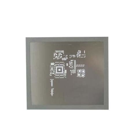
Modern PCB assembly relies on advanced SMT methodologies to address the complexities of BGA assembly and high-density PCB designs. Precision placement techniques, such as vision-guided robotic systems, ensure accurate component alignment, minimizing defects in PCBA workflows. Optimizing SMT processes involves balancing solder paste deposition, stencil design, and thermal profiling to achieve consistent results, particularly for fine-pitch BGA components.
Tip: Leverage real-time process monitoring during reflow soldering to detect thermal inconsistencies early, preventing latent failures in BGA connections.
Innovations like automated optical inspection (AOI) and X-ray inspection systems enhance quality control by identifying solder joint voids or misalignments invisible to the naked eye. Material advancements, including high-thermal-conductivity substrates, improve heat dissipation in densely packed PCBs, ensuring long-term reliability. Integrating smart manufacturing tools—such as IoT-enabled pick-and-place machines—streamlines PCBA production, reducing downtime through predictive maintenance.
For BGA assembly, advanced reflow soldering methods, such as nitrogen-assisted environments, mitigate oxidation and improve wetting, critical for robust interconnections. Additionally, modular SMT equipment allows flexible scaling, adapting to evolving PCB design requirements without overhauling production lines. These strategies collectively elevate manufacturing precision, throughput, and yield, positioning PCBA providers to meet the demands of next-generation electronics.

Introduction to Surface Mount Technology (SMT) in Modern PCBA
Surface Mount Technology (SMT) has revolutionized PCB assembly by enabling faster, more precise, and scalable manufacturing processes. Unlike traditional through-hole methods, SMT allows components to be mounted directly onto the surface of PCBs, significantly reducing board size while improving electrical performance. This approach is particularly critical in modern PCBA workflows, where high-density designs and miniaturized components like BGA (Ball Grid Array) packages demand exceptional placement accuracy. By leveraging automated pick-and-place systems, SMT ensures consistent alignment of micro-scale components, which is essential for maintaining signal integrity and thermal stability in complex electronic devices.
The integration of SMT into PCB assembly also addresses challenges such as component spacing and thermal management. For instance, advanced solder paste printing techniques ensure uniform deposition, minimizing defects during reflow soldering—a critical step for securing BGA connections. Additionally, the use of high-performance substrates and low-voiding solder alloys enhances reliability in harsh operating environments. As PCBA processes evolve, the synergy between SMT equipment and intelligent software further streamlines production, enabling real-time adjustments to placement accuracy and process parameters. This adaptability not only boosts yield rates but also supports the growing demand for compact, high-speed electronics across industries like automotive, telecommunications, and IoT.
By prioritizing precision and scalability, SMT remains the cornerstone of efficient PCB assembly, ensuring that modern PCBA workflows meet both performance benchmarks and cost-effectiveness goals.
Overcoming BGA Assembly Challenges with Precision Placement Techniques
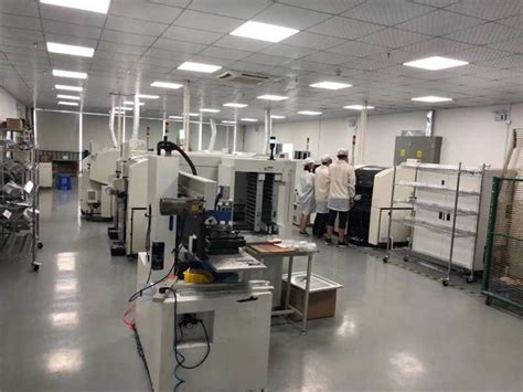
Achieving reliable BGA assembly in high-density PCBA demands meticulous attention to placement accuracy, thermal dynamics, and solder joint integrity. Modern Surface Mount Technology (SMT) leverages advanced vision systems, high-precision pick-and-place machines, and intelligent algorithms to address the inherent complexities of Ball Grid Array (BGA) components. These devices, characterized by their dense grid of solder balls beneath the package, require sub-micron alignment accuracy to ensure proper electrical connectivity and mechanical stability on the PCB. Thermal expansion mismatches between the BGA package and the substrate further complicate the process, necessitating precise control over solder paste deposition and reflow profiles.
Innovations in PCB assembly workflows now integrate real-time feedback mechanisms, such as laser-assisted component alignment and 3D solder paste inspection (SPI), to minimize placement errors. For instance, automated systems adjust placement pressure and angle dynamically, compensating for warpage or uneven surfaces on the PCB. Additionally, the use of no-clean fluxes and low-voiding solder pastes enhances joint reliability, particularly in applications exposed to thermal cycling or mechanical stress. Advanced SMT equipment also supports ultra-fine-pitch BGAs, enabling the integration of components with pitches as low as 0.3mm—a critical capability for next-generation electronics.
To mitigate risks like solder bridging or open connections, manufacturers adopt predictive modeling tools that simulate reflow behavior based on PCB material properties and component layouts. Pairing these simulations with closed-loop reflow ovens ensures consistent heating rates, reducing thermal gradients that could compromise BGA reliability. Furthermore, inline automated optical inspection (AOI) systems validate solder joint quality post-reflow, flagging defects such as insufficient wetting or voids before final PCBA testing.
By combining precision placement technologies with material science advancements, the industry continues to push the boundaries of BGA assembly efficiency and durability. These strategies not only enhance manufacturing yields but also align with the growing demand for compact, high-performance electronics in sectors like automotive, aerospace, and IoT.
Optimizing SMT Processes for High-Density PCB Integration
Achieving seamless integration of high-density PCB designs demands a meticulous approach to SMT (Surface Mount Technology) processes. As modern PCBA (Printed Circuit Board Assembly) workflows increasingly incorporate complex BGA (Ball Grid Array) components and ultra-fine-pitch devices, manufacturers must prioritize precision and adaptability. Central to this effort is the deployment of advanced automated pick-and-place systems equipped with vision-guided alignment, which ensures accurate component positioning even on densely populated boards. These systems minimize placement errors, a critical factor when handling BGA assembly, where misalignment can lead to costly rework or field failures.
Material selection plays an equally vital role. The use of low-voiding solder pastes with fine particle sizes enhances deposition accuracy during stencil printing, reducing the risk of bridging or insufficient joints in tight layouts. Additionally, optimizing reflow soldering profiles—tailored to the thermal characteristics of high-density PCB substrates—ensures uniform heat distribution. This is particularly crucial for BGA connections, where uneven thermal expansion can compromise solder joint integrity.
To address thermal management challenges inherent in compact designs, innovations in PCB substrates, such as high-Tg (glass transition temperature) materials or metal-core boards, improve heat dissipation without sacrificing routing density. Pairing these substrates with SMT-compatible thermal interface materials further enhances reliability in applications like automotive or industrial electronics.
Automation extends beyond placement and soldering. Automated optical inspection (AOI) and X-ray inspection systems are indispensable for verifying solder joint quality beneath BGA components, where visual checks are impractical. These systems integrate seamlessly into PCBA lines, enabling real-time defect detection and process adjustments.
Finally, smart manufacturing principles, including IoT-enabled SMT equipment, allow for data-driven optimization. By analyzing production metrics, such as placement speed or solder paste volume, manufacturers can fine-tune processes to balance throughput and precision—a necessity for scaling high-density PCB assembly without compromising yield. Through these strategies, PCBA workflows achieve the robustness required for next-generation electronics, where component density and performance demands continue to escalate.
Advanced Reflow Soldering Methods for Reliable BGA Connections
Modern PCB assembly processes demand precision in BGA (Ball Grid Array) soldering to ensure robust electrical and mechanical connections. Advanced reflow soldering techniques have become pivotal in achieving this, particularly for high-density PCBA designs. A critical innovation lies in dynamic temperature profiling, which tailors thermal curves to match specific PCB substrate materials and solder paste properties. By optimizing ramp rates, peak temperatures, and cooling gradients, manufacturers mitigate thermal stress on delicate components, reducing risks of warping or solder joint fractures.
The integration of nitrogen-enriched reflow ovens further enhances reliability by minimizing oxidation during soldering. This is especially vital for BGA assembly, where even minor oxide formation can compromise interconnect integrity. Additionally, laser-assisted localized heating enables targeted energy application, ideal for mixed-technology boards combining SMT (Surface Mount Technology) components with heat-sensitive devices. Such methods ensure consistent solder reflow without overheating adjacent elements.
To address challenges in high-density PCB integration, vacuum reflow systems have emerged. These systems eliminate trapped air pockets in solder joints, a common issue with fine-pitch BGAs, ensuring void-free connections critical for high-frequency or power-intensive applications. Pairing these advancements with real-time thermal monitoring sensors allows for closed-loop control, dynamically adjusting parameters to maintain process stability.
Material compatibility is another focus area. Low-voiding solder pastes, formulated with nano-coated particles, improve wetting behavior during reflow, enhancing joint strength and electrical conductivity. When combined with predictive analytics for profile optimization, these materials elevate PCBA yields while reducing post-assembly defects.
Finally, post-reflow inspection techniques like 3D X-ray imaging and automated optical inspection (AOI) validate solder joint quality, ensuring compliance with stringent industry standards. Together, these innovations in reflow soldering not only streamline PCB assembly workflows but also reinforce the reliability of complex BGA-based electronics in demanding environments.
Automated Inspection Systems for Enhanced SMT Quality Control
Modern PCB assembly relies heavily on automated inspection systems to ensure precision and reliability in SMT-driven processes. As PCBA designs grow more complex—particularly with high-density BGA components—traditional manual inspection methods fall short in detecting microscopic defects such as solder bridging, insufficient paste deposition, or misaligned components. Advanced optical inspection tools, including Automated Optical Inspection (AOI) and X-ray inspection, have become indispensable for maintaining stringent quality standards. AOI systems employ high-resolution cameras and machine learning algorithms to scan PCB surfaces, identifying deviations from design specifications in real time. For BGA assembly, where solder joints are hidden beneath components, X-ray imaging provides non-destructive internal visualization, enabling manufacturers to verify joint integrity and alignment without disassembly.
Integrating these systems into SMT workflows ensures continuous feedback loops, allowing immediate corrections during PCBA production. For instance, AOI data can trigger adjustments in stencil printing or component placement machines, minimizing rework and reducing material waste. Similarly, inline X-ray inspection paired with thermal profiling optimizes reflow soldering parameters for BGA reliability. By leveraging statistical process control (SPC), manufacturers can correlate inspection data with process variables, further refining PCB integration and assembly consistency. The result is a streamlined PCBA manufacturing chain where defects are caught early, throughput is maximized, and end-product performance aligns with the demands of next-generation electronics.

Material Innovations in PCB Substrates for Thermal Management
Effective thermal management is critical in modern PCB assembly, particularly as PCBA designs incorporate high-density components like BGA packages and advanced SMT configurations. Innovations in substrate materials are addressing heat dissipation challenges, ensuring reliability in demanding applications. Traditional FR-4 substrates, while cost-effective, struggle with thermal conductivity, leading to hotspots and reduced performance in compact PCB layouts.
Recent advancements focus on metal-core substrates (e.g., aluminum or copper bases) and ceramic-filled laminates, which enhance heat transfer while maintaining electrical insulation. For instance, aluminum-based substrates achieve thermal conductivity values up to 8 W/mK, compared to FR-4’s 0.3 W/mK, significantly reducing thermal resistance in BGA assembly environments. Additionally, thermally conductive prepregs and high-Tg (glass transition temperature) materials improve stability during reflow soldering, minimizing warpage and ensuring consistent solder joint integrity.
| Material Type | Thermal Conductivity (W/mK) | Key Advantages |
|---|---|---|
| FR-4 | 0.3 | Low cost, widely available |
| Metal-Core (Aluminum) | 8.0 | High heat dissipation, mechanical strength |
| Ceramic-Filled Laminates | 2.5–4.0 | Balanced thermal/electrical performance |
| High-Tg Epoxy Resins | 0.5–1.0 | Enhanced thermal stability, reduced warpage |
These innovations enable PCB assembly workflows to integrate SMT components more densely without compromising thermal performance. For example, embedded cooling channels within multilayer PCBs direct heat away from BGA arrays, while silicon-based thermal interface materials (TIMs) bridge gaps between components and heat sinks. Such advancements are critical for applications like automotive electronics and 5G infrastructure, where PCBA reliability under thermal stress is non-negotiable.
By leveraging these material breakthroughs, manufacturers achieve higher yield rates and longer operational lifespans, aligning with the industry’s push toward miniaturization and energy efficiency.
Streamlining PCBA Workflows with Smart SMT Equipment Integration
Integrating intelligent SMT equipment into PCBA production lines has become a cornerstone for achieving efficiency and precision in modern electronics manufacturing. Advanced pick-and-place systems, enhanced by machine vision and AI-driven algorithms, enable rapid component positioning with micron-level accuracy, critical for handling fine-pitch BGA packages and high-density PCB layouts. By synchronizing design data with production machinery, manufacturers reduce setup times and minimize human intervention, ensuring seamless transitions from prototyping to mass production.
Central to this integration is the adoption of closed-loop feedback systems that monitor process variables such as solder paste deposition, component alignment, and thermal profiles during reflow. These systems dynamically adjust parameters to maintain consistency across batches, addressing challenges like warpage in large PCB assemblies or void formation in BGA solder joints. Additionally, modular SMT lines equipped with interoperable software platforms allow real-time data sharing between stencil printers, placement machines, and inspection tools, creating a cohesive workflow that accelerates throughput without compromising quality.
The use of predictive maintenance tools further optimizes equipment uptime, analyzing vibration, temperature, and wear patterns to preemptively flag potential failures. This proactive approach, combined with IoT-enabled diagnostics, ensures uninterrupted production cycles—a critical factor for industries demanding high-reliability PCBA outputs. By harmonizing hardware precision with data-driven intelligence, manufacturers achieve tighter process control, reduced material waste, and faster time-to-market for complex electronics leveraging BGA technologies and multilayer PCB architectures.
Future Trends in SMT and BGA Assembly for Next-Gen Electronics
The evolution of PCB assembly technologies continues to reshape the landscape of PCBA manufacturing, with emerging trends emphasizing precision, scalability, and sustainability. As next-generation electronics demand higher component density and faster processing, advanced SMT techniques are integrating artificial intelligence (AI) and machine learning to optimize BGA assembly accuracy. These systems now leverage real-time data analytics to adjust placement parameters dynamically, minimizing errors in high-density PCB layouts. Additionally, the rise of 3D-printed solder paste stencils and hybrid reflow ovens is enhancing thermal uniformity, critical for reliable BGA connections in complex multilayer boards.
Material science breakthroughs are also driving progress, with novel substrates offering improved thermal management and reduced signal loss. Innovations like embedded passive components and ultra-low-loss dielectrics enable tighter integration of SMT components, addressing challenges posed by shrinking form factors. Meanwhile, smart manufacturing frameworks are streamlining PCBA workflows through interconnected SMT equipment, enabling seamless communication between pick-and-place machines, inspection systems, and reflow ovens. This integration reduces cycle times while ensuring traceability across the production line.
Sustainability is emerging as a key focus, with manufacturers adopting lead-free solder alloys and recyclable PCB materials to meet environmental regulations. Furthermore, advancements in automated optical inspection (AOI) and X-ray systems are elevating quality control standards, detecting micro-voids in BGA joints with submicron precision. As the industry shifts toward IoT-enabled devices and 5G infrastructure, these trends will solidify PCB assembly as a cornerstone of reliable, high-performance electronics manufacturing.
Conclusion
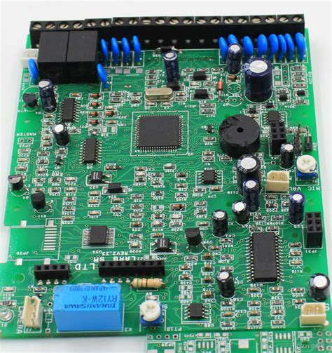
The evolution of PCB assembly has been significantly shaped by advancements in Surface Mount Technology (SMT), particularly in addressing the complexities of BGA assembly and high-density PCB integration. Modern PCBA workflows now leverage precision placement systems, adaptive reflow soldering, and intelligent automation to achieve unprecedented accuracy in component mounting and solder joint reliability. These innovations not only enhance manufacturing efficiency but also ensure robust thermal and electrical performance, even in densely packed layouts.
Central to this progress is the integration of automated optical inspection (AOI) systems, which mitigate defects in BGA connections by providing real-time feedback during SMT processes. Coupled with material advancements in PCB substrates—such as high-thermal-conductivity laminates—manufacturers can now better manage heat dissipation, a critical factor in sustaining long-term device reliability. Furthermore, smart equipment interoperability enables seamless data exchange across PCBA production stages, reducing bottlenecks and accelerating time-to-market.
As industries push toward miniaturization and higher performance, the synergy between SMT techniques and BGA optimization remains pivotal. By prioritizing precision, scalability, and material science, the PCB assembly sector is poised to meet the demands of next-generation electronics while maintaining stringent quality standards. These strategies collectively underscore the importance of continuous innovation in sustaining competitive advantage across evolving technological landscapes.
FAQs
What role does SMT play in modern PCB assembly?
Surface Mount Technology (SMT) enables high-speed, high-precision placement of components like BGA packages onto PCBs, reducing manual errors and improving throughput in PCBA workflows. Its compatibility with miniaturized designs supports high-density PCB integration.
How do precision placement techniques address BGA assembly challenges?
Advanced SMT equipment uses vision systems and laser alignment to ensure accurate BGA ball-grid positioning. This minimizes voids and misalignment, critical for reliable solder joints in high-performance PCBA applications.
What innovations enhance thermal management in PCB substrates?
Modern PCB assembly leverages materials like metal-core substrates and high-Tg laminates to dissipate heat efficiently. These substrates improve reliability in BGA-heavy designs, especially for applications requiring prolonged thermal cycling.
Why are automated inspection systems vital for SMT quality control?
Automated optical (AOI) and X-ray (AXI) inspection systems detect defects such as solder bridging or incomplete BGA connections early in the PCBA process, reducing rework costs and ensuring compliance with industry standards.
How does smart equipment integration streamline PCBA workflows?
IoT-enabled SMT machines collect real-time data on placement accuracy and solder profiles, enabling predictive maintenance and process optimization. This integration minimizes downtime and boosts yield in large-scale PCB assembly.
What future trends are shaping SMT and BGA assembly?
Emerging trends include 3D-printed electronics for complex PCB geometries and AI-driven process optimization for defect prediction. These advancements aim to further enhance precision and scalability in next-gen PCBA manufacturing.
Ready to Optimize Your PCB Assembly Process?
For tailored solutions in advanced PCBA and BGA assembly, please click here to explore our expertise and cutting-edge manufacturing capabilities.


