Advanced Strategies for Efficient 6-Layer PCB Manufacturing

Key Takeaways
When planning 6-layer PCB manufacturing, understanding core optimization strategies ensures your design meets performance and cost targets. Start by evaluating stackup configurations—balanced arrangements with dedicated signal, power, and ground layers minimize noise while improving thermal management. For high-density layouts, Via-in-Pad techniques reduce parasitic inductance, enabling tighter component placement without sacrificing reliability.
Tip: Collaborate early with PCB manufacturing companies to validate material choices (e.g., low-loss FR-4 or Rogers substrates) that align with your application’s thermal and electrical demands.
Critical signal paths benefit from 4-wire testing, a precision method for verifying trace resistance and continuity. This becomes essential in wearables and IoT devices, where compact 6-layer PCBs demand flawless signal integrity. To accelerate development cycles, consider rapid prototyping services—many manufacturers now offer 48-hour turnaround for functional validation.
| Factor | Impact on PCB Manufacturing Cost | Optimization Strategy |
|---|---|---|
| Layer Count | Increases material and lamination expenses | Use hybrid stackups (mixed dielectrics) |
| Via Types | Microvias add complexity | Limit blind/buried vias to critical zones |
| Testing | 4-wire methods raise labor time | Automate testing protocols |
Balancing PCB manufacturing business priorities requires addressing EMI risks through strategic layer pairing and shielding. Dedicated power planes in 6-layer designs not only stabilize voltage distribution but also reduce loop inductance by 30–40% compared to split-plane configurations. Always model current return paths during layout to avoid unexpected interference.
For cost-sensitive projects, negotiate volume discounts with PCB manufacturing partners while standardizing materials and finish options. This approach maintains quality without inflating per-unit expenses—a critical consideration for scaling production.

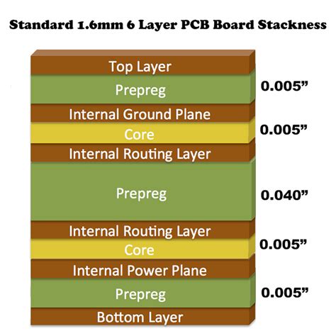
Optimizing 6-Layer PCB Stackup Configurations
When designing 6-layer PCBs, your stackup configuration directly impacts performance, PCB manufacturing cost, and production timelines. Start by defining clear layer functions: typical arrangements place high-speed signal layers adjacent to ground planes to minimize interference while isolating power planes. For compact wearables, use thinner prepreg materials (≤3 mil) to reduce overall thickness without compromising impedance control.
Leading PCB manufacturing companies recommend symmetrical stackups to prevent warping during thermal cycles—a critical factor for high-reliability systems. Incorporate via-in-pad techniques early in the design phase to save space, but verify compatibility with your fabricator’s capabilities. For instance, microvia filling processes may require specialized equipment, affecting both timelines and PCB manufacturing business workflows.
To balance cost and performance, prioritize critical signal layers over general-purpose routing. Pairing a 2-2-2 stackup with hybrid materials (e.g., FR-4 mixed with high-speed substrates) can enhance signal integrity while keeping PCB manufacturing expenses manageable. Always simulate thermal and mechanical stress profiles before finalizing the design—this preemptive step avoids costly revisions post-prototyping. By aligning your stackup strategy with fabrication realities, you ensure scalability across low-to-high-volume production runs.
Via-in-Pad Techniques for High-Density Routing
When designing 6-layer PCBs for compact wearables or high-speed systems, via-in-pad techniques address routing challenges in space-constrained layouts. By embedding vias directly into component pads, you reduce trace lengths and eliminate the need for dog-bone fanouts, freeing up 15–20% of board real estate. High-density interconnects (HDIs) benefit particularly from this approach, as it minimizes impedance discontinuities in high-frequency signal paths—a critical factor for PCB manufacturing of advanced IoT devices or miniaturized medical sensors.
However, PCB manufacturing companies often highlight thermal management as a key consideration. Filling vias with conductive epoxy or copper plating prevents solder wicking during reflow, ensuring reliable electrical connections. For designs requiring blind or buried vias, precise laser drilling becomes essential, which may impact PCB manufacturing cost by 8–12% depending on layer alignment tolerances.
To balance performance and affordability, prioritize via-in-pad for BGA packages or QFN components where signal integrity outweighs incremental cost increases. Partnering with experienced PCB manufacturing business providers ensures proper DFM checks, such as pad diameter-to-drill ratios and solder mask alignment, to avoid yield losses in volume production. This approach becomes critical when scaling prototypes into mass-market solutions without compromising routing density or electrical performance.

4-Wire Testing for Reliable Signal Integrity
When designing complex 6-layer PCBs, ensuring signal integrity becomes critical—especially in high-speed or mixed-signal systems. 4-wire testing (Kelvin sensing) addresses this by eliminating lead resistance errors during impedance measurements, a common pitfall in traditional 2-wire methods. By separating current-carrying and voltage-sensing paths, you achieve <1% measurement accuracy for trace resistance, even in PCB manufacturing scenarios with ultra-thin copper layers (≤½ oz).
Leading PCB manufacturing companies integrate this technique during electrical testing phases to validate high-frequency interconnects and power plane stability. For instance, verifying impedance matching in differential pairs or detecting micro-voids in via fills becomes more reliable, directly impacting PCB manufacturing cost by reducing post-production failures. While the process adds ~15% to initial testing time, it prevents costly redesigns in applications like 5G modules or IoT controllers.
To optimize this approach, pair 4-wire testing with temperature-controlled environments to minimize thermal EMF effects. Modern test fixtures now automate probe positioning for dense layouts, ensuring compatibility with PCB manufacturing business models prioritizing rapid validation. By adopting these protocols, you maintain signal fidelity across GHz-range circuits while balancing precision and scalability in multilayer production.

Rapid Prototyping -Hour PCB Fabrication
When transitioning from design validation to functional prototyping, PCB manufacturing timelines often dictate project viability. Leading PCB manufacturing companies now offer 48-hour turnaround for 6-layer boards, leveraging automated optical inspection (AOI) and laser direct imaging (LDI) to reduce manual processing. This acceleration enables rapid iteration for high-density wearables or IoT devices, where even minor layout adjustments can impact antenna performance or power efficiency.
To minimize PCB manufacturing cost during prototyping, prioritize panelization strategies that maximize material use while adhering to your fabricator’s design-for-manufacturability (DFM) guidelines. For instance, via-in-pad placements in BGA-driven designs often require sequential lamination—a step that benefits from pre-validated stackup templates. Advanced shops combine these templates with 4-wire Kelvin testing to preempt impedance mismatches, ensuring first-article success rates above 90%.
In high-stakes PCB manufacturing business environments, this speed-to-market approach balances technical rigor with economic pragmatism. By aligning your prototyping workflow with suppliers offering 24/7 engineering support, you mitigate risks of delayed product launches while preserving budget for volume production optimizations.
6-Layer PCBs for Compact Wearable Applications
When designing PCB manufacturing solutions for compact wearables, balancing miniaturization with performance becomes critical. A 6-layer stackup allows you to integrate dedicated signal, power, and ground layers while maintaining a footprint under 25mm²—ideal for smartwatches or medical sensors. By optimizing layer assignments, you can isolate sensitive RF circuits from noisy digital components, reducing crosstalk by up to 40% compared to 4-layer designs.
Advanced PCB manufacturing companies leverage via-in-pad techniques and 0.1mm laser-drilled microvias to route high-speed signals efficiently in constrained spaces. This approach minimizes parasitic inductance, ensuring stable power delivery even in ultra-thin wearables. However, tighter tolerances and specialized materials like flexible polyimide substrates may increase PCB manufacturing cost by 15-20%, requiring careful trade-off analysis during prototyping.
To maintain profitability in the PCB manufacturing business, consider hybrid designs that combine rigid and flex layers, reducing assembly steps for curved wearable housings. Automated optical inspection (AOI) and impedance-controlled routing further ensure reliability in dynamic environments. Pairing these strategies with thermal management layers—such as embedded copper pours—helps dissipate heat from densely packed components, extending device lifespan without compromising form factor.
Cost-Effective Multilayer Manufacturing Strategies
Balancing performance and PCB manufacturing cost requires strategic planning at every stage. Start by optimizing material selection—high-Tg FR-4 laminates offer thermal stability without premium pricing, while standardized dielectric thicknesses reduce custom PCB manufacturing fees. To minimize layer count complexities, adopt impedance-controlled routing early in the design phase, which avoids costly post-fabrication adjustments. Partnering with PCB manufacturing companies that offer volume-tiered pricing can lower per-unit expenses, especially for wearable or IoT devices requiring mid-to-high production runs.
Automation plays a pivotal role: laser-direct imaging (LDI) systems achieve tighter tolerances for high-density interconnects, reducing scrap rates by up to 30%. For prototypes, leverage rapid-turn services that align with your PCB manufacturing business timelines—many suppliers now provide 48-hour cycles without sacrificing testing rigor. However, avoid over-specifying finishes; ENIG (Electroless Nickel Immersion Gold) suits most wearables, while HASL (Hot Air Solder Leveling) remains cost-effective for consumer electronics.
Finally, implement design-for-manufacturing (DFM) checks to flag issues like insufficient annular rings or asymmetric copper distribution, which often lead to rework charges. By aligning your design choices with production-scale capabilities, you maintain PCB manufacturing cost efficiency without compromising signal integrity or reliability in complex 6-layer systems.
EMI Mitigation in Advanced 6-Layer Designs
When designing 6-layer PCBs for high-frequency applications, managing electromagnetic interference (EMI) becomes critical to ensure reliable performance. Start by optimizing your layer stackup—placing power and ground planes adjacent to signal layers creates natural shielding. For example, a common configuration pairs Signal-Ground-Power-Signal-Ground-Signal layers, which minimizes cross-talk while providing low-impedance return paths.
PCB manufacturing companies often recommend ground stitching vias around high-speed traces to reduce loop areas and suppress radiated emissions. Integrating shielding cans or ferrite beads near noise-generating components like oscillators further isolates disruptive signals. To balance PCB manufacturing cost, prioritize critical areas requiring EMI suppression rather than applying uniform shielding across the entire board.
For sensitive circuits, use impedance-controlled routing and avoid abrupt trace bends that can cause reflections. Pair this with guard traces or copper pours to contain electromagnetic fields. When collaborating with PCB manufacturing partners, verify their capability to implement laser-drilled microvias for precise grounding structures without compromising layer alignment.
Finally, validate designs through pre-production EMI simulations and post-fabrication testing. While these steps may add complexity to the PCB manufacturing business, they prevent costly redesigns and ensure compliance with regulatory standards for applications like IoT devices or automotive systems.
Integrating Power Planes in 6-Layer Systems
When designing power distribution for 6-layer PCBs, you must prioritize low-impedance paths and thermal management. A typical stackup places dedicated power planes on layers 2 and 5, sandwiched between signal layers and ground planes. This configuration minimizes voltage drops while shielding high-speed traces from interference. Via-in-pad techniques prove critical here, allowing direct connections between surface-mounted components and internal power layers without compromising routing density—a key advantage for pcb manufacturing companies tackling complex wearables or IoT devices.
To reduce inductance, pair power planes with adjacent ground layers, creating a distributed decoupling effect. For multi-voltage designs, split power planes require precise copper balancing to avoid warping during lamination—a factor influencing pcb manufacturing cost. Advanced fabricators use simulation tools to predict current flow and optimize plane shapes, ensuring uniform thermal dissipation. When selecting materials, high-Tg FR4 or specialized laminates may offset heat buildup in compact systems, though this impacts overall pcb manufacturing business logistics.
Always validate power integrity through 4-wire resistance testing post-fabrication, particularly at plane transitions. This step ensures your design meets the reliability standards demanded by high-performance applications while maintaining cost-efficiency in pcb manufacturing.
Conclusion
When navigating PCB manufacturing for complex 6-layer designs, balancing technical precision with PCB manufacturing cost considerations becomes critical. Reputable PCB manufacturing companies leverage advanced stackup configurations and Via-in-Pad integration to address high-density routing challenges while maintaining signal integrity. By adopting 4-wire testing protocols during fabrication, you ensure reliable performance—especially for applications like wearables or high-speed systems where margin for error is minimal.
For businesses scaling their PCB manufacturing business, rapid prototyping services (often within 48 hours) enable faster iteration cycles without compromising quality. However, optimizing layer utilization and material selection remains paramount to avoid unnecessary expenses. As you finalize designs, prioritize collaboration with manufacturers to align EMI mitigation strategies with production capabilities. This approach not only streamlines workflows but also safeguards against costly redesigns. Ultimately, success in multilayer fabrication hinges on merging innovative engineering with cost-effective supply chain partnerships—ensuring your 6-layer PCBs meet both technical specifications and budgetary constraints.
Frequently Asked Questions
How does PCB manufacturing complexity change with 6-layer designs?
Six-layer boards require precise stackup configurations and material selection to balance signal integrity and thermal management. While PCB manufacturing companies often charge more for multilayer designs, optimized layer planning reduces PCB manufacturing cost by minimizing material waste and rework.
What design choices impact PCB manufacturing business timelines?
Techniques like Via-in-Pad and 4-wire testing add precision but may extend production cycles. Partnering with manufacturers offering rapid prototyping (e.g., 48-hour turnarounds) ensures faster validation for wearables or IoT systems without compromising quality.
Can 6-layer PCBs reduce EMI in compact devices?
Yes. Proper power plane integration and shielding layers in the stackup suppress electromagnetic interference. Many PCB manufacturing providers now use advanced simulation tools to pre-validate designs, lowering risks before fabrication.
How do I evaluate PCB manufacturing companies for multilayer projects?
Prioritize vendors with expertise in high-density interconnect (HDI) processes and certifications like ISO 9001. Request detailed breakdowns of PCB manufacturing cost drivers, including material grades, via types, and testing protocols.
Ready to Optimize Your 6-Layer PCB Project?
For tailored solutions that balance performance and PCB manufacturing cost, please click here to consult experts specializing in advanced multilayer fabrication.


