Advanced Strategies for High-Volume Industrial PCB Assembly Production
Key Takeaways
When scaling PCB assembly for industrial applications, manufacturers must balance precision, speed, and adaptability. First and foremost, automation-driven workflows form the backbone of high-volume PCBA production. By integrating advanced robotic placement systems and AI-powered optical inspection, facilities can achieve throughput rates exceeding 95,000 components per hour while maintaining sub-10 ppm defect levels.
A critical differentiator lies in modular manufacturing architectures, which allow rapid reconfiguration of PCB assembly lines for diverse product batches. This approach reduces changeover downtime by 40–60% compared to fixed-line setups, as demonstrated in recent implementations by Tier 1 automotive suppliers.
| Strategy | Traditional Approach | Modern Optimization |
|---|---|---|
| Quality Assurance | Manual sampling (5–10%) | Automated AOI (100% coverage) |
| Thermal Management | Post-production testing | Simulation-driven design |
| Material Utilization | 82–88% efficiency | 94–97% via AI nesting |
Equally important is the shift toward closed-loop process control in PCBA manufacturing. Real-time data from IoT-enabled pick-and-place machines and reflow ovens enables micro-adjustments to solder paste application and thermal profiles, reducing rework rates by up to 32%. For mission-critical industrial applications, this aligns with the growing emphasis on predictive maintenance models that analyze component stress patterns to preempt field failures.
Cost optimization in high-volume PCB assembly increasingly relies on dynamic resource allocation algorithms. These systems automatically balance workload across parallel SMT lines, mitigating bottlenecks during peak demand cycles. When paired with vendor-managed inventory programs for high-turnover components, manufacturers report 18–25% reductions in carrying costs without compromising production continuity.
The convergence of these strategies underscores a fundamental truth: industrial-scale PCBA excellence requires treating manufacturing not as a linear process, but as a continuously evolving ecosystem. This paradigm shift enables manufacturers to meet tightening IPC-A-610 Class 3 specifications while maintaining profit margins in competitive markets.
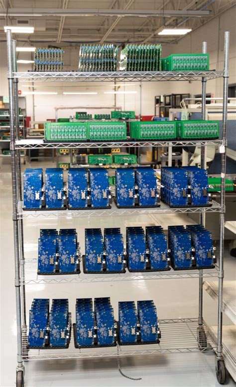
Automating Industrial PCB Assembly for Scalability
Modern PCB assembly workflows increasingly rely on advanced automation to meet the demands of high-volume production while maintaining precision. Robotic pick-and-place systems, for instance, have revolutionized component placement by achieving accuracies within ±25 microns—critical for densely packed PCBA designs in industrial applications. These systems integrate machine vision to verify component orientation and solder paste application, reducing human error by over 70% in complex assemblies.
Scalability in industrial PCB assembly hinges on modular production lines that adapt to fluctuating order volumes without compromising throughput. For example, dual-lane conveyor systems paired with automated optical inspection (AOI) enable parallel processing of boards, cutting cycle times by 40% compared to traditional single-lane setups. Manufacturers further enhance flexibility by deploying collaborative robots (cobots) for tasks like board handling or rework, which can be reprogrammed in under two hours for new product variants.
A key advantage of automation lies in data-driven process optimization. Sensors embedded in surface-mount technology (SMT) equipment collect real-time metrics on solder joint quality or thermal profiles, feeding into AI-powered analytics platforms. This closed-loop feedback allows immediate adjustments to reflow oven temperatures or stencil pressure, ensuring consistent PCBA output even during 24/7 production runs.
However, achieving true scalability requires harmonizing hardware with enterprise resource planning (ERP) systems. Automated material tracking via RFID tags, for instance, synchronizes component inventories with assembly schedules, preventing line stoppages due to part shortages. Such integration reduces material waste by up to 18% in high-mix environments.
By implementing these strategies, manufacturers create PCB assembly ecosystems where throughput and precision scale proportionally—a critical foundation for the subsequent phase of rigorous quality control.
Implementing Rigorous Quality Control in PCB Production
In high-volume industrial PCB assembly, maintaining consistent quality requires a multilayered approach that integrates advanced inspection technologies, standardized protocols, and data-driven process adjustments. Modern PCBA manufacturing leverages automated optical inspection (AOI) systems equipped with high-resolution cameras and machine learning algorithms to detect micro-scale defects like solder bridging or component misalignment. These systems analyze millions of data points per board, ensuring deviations are flagged before progressing to subsequent stages.
Tip: Implement statistical process control (SPC) tools to monitor critical parameters such as solder paste volume and reflow oven temperature in real time. This proactive approach minimizes variability and reduces post-production rework.
For mission-critical applications, X-ray inspection becomes indispensable. This non-destructive method identifies hidden flaws in ball grid array (BGA) components or internal layer connections, which are common pain points in dense PCB assembly designs. Pairing these techniques with in-circuit testing (ICT) and functional testing (FCT) validates electrical performance under simulated operating conditions, ensuring boards meet industrial-grade reliability benchmarks.
Material traceability is another cornerstone of robust quality control. By embedding unique identifiers like barcodes or QR codes into each PCBA, manufacturers can track components back to their origin, batch numbers, and storage conditions. This granular visibility is vital for root cause analysis during failure investigations and aligns with ISO 9001 and IPC-A-610 compliance requirements.
Suggestion: Adopt a closed-loop feedback system where test results automatically trigger adjustments in upstream processes. For example, recurring solder voids detected by AOI could prompt recalibration of stencil printers or reflow profiles.
Finally, fostering a zero-defect culture through regular cross-functional audits and operator training ensures human expertise complements technological safeguards. By harmonizing automated precision with meticulous oversight, manufacturers achieve the scalability and cost-efficiency demanded by industrial PCB assembly without compromising on quality.
Cost-Efficient Strategies for High-Volume PCB Manufacturing
Achieving cost efficiency in industrial PCB assembly requires balancing economies of scale with precision engineering. For manufacturers targeting high-volume production, optimizing material utilization forms the foundation of savings. Bulk purchasing of FR-4 substrates, copper-clad laminates, and standardized components can reduce per-unit costs by 12–18%, while maintaining compatibility with PCBA workflows. However, cost-cutting must not compromise performance—adopting design-for-manufacturing (DFM) principles early in product development minimizes material waste and avoids costly redesigns during scaling.
Automation plays a pivotal role in driving down expenses. Integrating PCB assembly lines with pick-and-place robotics and reflow soldering systems reduces labor dependency and ensures consistent throughput. For example, a single automated surface-mount technology (SMT) line can place 25,000 components per hour with ±0.025mm accuracy, slashing error-related rework costs by up to 40%. Pairing this with predictive maintenance algorithms further curtails downtime, ensuring machinery operates at peak efficiency across 24/7 production cycles.
Process optimization extends beyond the factory floor. Implementing just-in-time (JIT) inventory management for PCBA materials reduces storage overheads and mitigates obsolescence risks, particularly for fast-evolving industrial IoT applications. Additionally, advanced thermal profiling during soldering phases minimizes energy consumption while ensuring reliable interconnects—a critical factor for high-reliability industrial boards exposed to harsh environments.
Strategic partnerships with component suppliers and contract manufacturers can unlock further savings. Multi-year pricing agreements for high-demand ICs and connectors stabilize costs, while outsourcing non-core PCB assembly stages (e.g., conformal coating or final testing) allows manufacturers to focus capital on core competencies. Crucially, every cost-saving measure must align with ISO 9001 and IPC-A-610 standards to prevent quality trade-offs that erode long-term profitability.
By harmonizing scalable automation, lean material management, and collaborative supply chains, manufacturers transform industrial PCB assembly into a competitive advantage—delivering ruggedized, high-performance boards at prices that support mass adoption in automation, energy, and transportation sectors.
Ensuring Reliability in Industrial-Grade PCB Assembly
Achieving reliability in industrial PCB assembly demands a holistic approach that balances material science, precision engineering, and stringent validation protocols. At the core of dependable PCBA lies the selection of high-performance substrates and temperature-resistant components, which form the foundation for boards capable of enduring harsh industrial environments. For applications ranging from factory automation to power grid systems, PCB assemblies must withstand thermal cycling, mechanical stress, and prolonged exposure to contaminants like dust or moisture.
Advanced conformal coating techniques play a pivotal role in safeguarding circuits, with materials such as acrylics or silicones providing tailored protection against environmental factors. Manufacturers are increasingly adopting automated optical inspection (AOI) systems paired with X-ray verification to detect micro-scale defects—from solder joint voids to trace fractures—that could compromise long-term performance. These tools enable scalable quality assurance without sacrificing production throughput, a critical balance in high-volume manufacturing.
Thermal management strategies further elevate reliability, particularly for industrial-grade PCBAs handling high power loads. Engineers optimize copper weight distribution and incorporate thermal vias to dissipate heat efficiently, while accelerated life testing simulates decades of operational stress within controlled laboratory conditions. Compliance with standards like IPC-A-610 (Class 3) ensures assemblies meet the rigorous demands of aerospace, medical, or heavy machinery applications.
To maintain consistency across production batches, leading manufacturers implement statistical process control (SPC), monitoring variables such as solder paste viscosity and reflow oven temperature profiles. This data-driven approach minimizes deviations, ensuring every PCB assembly aligns with predefined reliability thresholds. As industrial systems grow more interconnected, edge-case scenario testing has become indispensable, validating performance under extreme voltage fluctuations or electromagnetic interference.
The integration of failure mode and effects analysis (FMEA) during design phases proactively addresses potential weaknesses, while traceability systems track components from sourcing to final integration. This end-to-end visibility not only strengthens reliability but also accelerates root cause analysis if field issues emerge, reinforcing trust in industrial PCB assembly solutions.
Advanced Robotics in PCB Manufacturing Workflows
The integration of advanced robotics into PCB assembly workflows has become a game-changing force for manufacturers targeting high-volume production. Modern robotic systems now handle tasks ranging from precision component placement to real-time defect detection, significantly enhancing both speed and accuracy in PCBA processes. Collaborative robots (cobots), for instance, work alongside human operators to manage repetitive tasks like solder paste application or connector installation, reducing cycle times by up to 40% while maintaining micron-level tolerances.
A key innovation lies in autonomous material handling systems, which streamline the movement of substrates between stations. These robots leverage machine vision to adapt to varying board geometries, ensuring seamless transitions in mixed-product environments. For industrial PCB assembly, this adaptability is critical when balancing diverse product lines—such as automotive control modules and industrial IoT sensors—within a single facility.
Moreover, AI-driven robotic inspection platforms are redefining quality assurance. Equipped with hyperspectral imaging and thermal profiling capabilities, these systems identify micro-scale soldering defects or component misalignments that traditional methods might miss. By integrating such technologies into PCBA workflows, manufacturers achieve near-zero defect rates even at production scales exceeding 100,000 units monthly.
The scalability of robotic systems also addresses labor-intensive bottlenecks. For example, adaptive pick-and-place robots can be reprogrammed in minutes to accommodate design changes, eliminating downtime during product transitions. This flexibility, combined with predictive maintenance algorithms, ensures continuous uptime—a vital factor for industries requiring just-in-time delivery, such as aerospace or medical device manufacturing.
As robotics evolve, their synergy with IoT-enabled analytics platforms creates a closed-loop manufacturing ecosystem. Data from robotic workflows feed into central systems, enabling dynamic adjustments to optimize throughput or material usage. For industrial-grade PCBA, this fusion of hardware and digital intelligence isn’t merely an upgrade—it’s becoming a strategic imperative to meet escalating demands for reliability and cost-efficiency.
Streamlining High-Volume PCB Assembly Processes
Efficiently managing PCB assembly workflows in high-volume industrial production requires a strategic blend of process optimization and technology integration. At the core of streamlining lies the adoption of modular design principles, which standardize component layouts and reduce variability across batches. By aligning PCBA designs with automated placement systems, manufacturers minimize manual interventions, accelerating throughput while maintaining precision.
A critical step involves implementing closed-loop feedback systems between surface-mount technology (SMT) lines and quality inspection stations. Real-time data from automated optical inspection (AOI) and X-ray testing devices enables immediate adjustments to solder paste application or component alignment, reducing rework rates by up to 40% in multi-layer board production. This approach not only enhances yield but also ensures compliance with industrial-grade reliability standards.
Equally critical is the synchronization of material logistics with assembly cycles. Just-in-time delivery of components, paired with smart inventory tracking powered by RFID or IoT-enabled systems, prevents bottlenecks in high-mix PCB assembly environments. For instance, integrating enterprise resource planning (ERP) software with manufacturing execution systems (MES) allows dynamic rerouting of work orders during unexpected component shortages.
Another cornerstone is the use of predictive maintenance algorithms for assembly machinery. By analyzing vibration patterns and thermal signatures in pick-and-place robots, manufacturers preemptively address wear in high-speed PCBA lines, achieving 95%+ equipment uptime. This proactive maintenance strategy proves vital when scaling to production volumes exceeding 50,000 units per batch.
To further streamline workflows, leading manufacturers deploy unified digital twins that simulate entire PCB assembly processes before physical production begins. These virtual models identify potential conflicts in panelization strategies or thermal profiles, enabling optimization of cycle times and energy consumption. When combined with adaptive conveyor systems that self-adjust to board dimensions, such innovations reduce changeover intervals by 30–60%, a decisive advantage in high-volume contract manufacturing.
Optimizing Thermal Management for Durable PCB Outputs
Effective thermal management is a cornerstone of producing reliable PCB assembly outputs for industrial applications. As power densities increase in modern electronics, managing heat dissipation becomes critical to preventing premature component failure and ensuring long-term durability. In high-volume PCBA production, thermal stress accumulates across solder joints, traces, and integrated circuits, making systematic heat mitigation strategies essential.
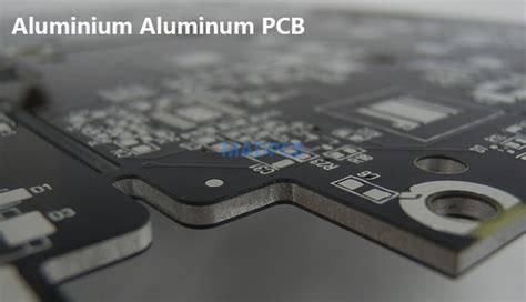
Advanced material selection forms the first line of defense. Using substrates with higher glass transition temperatures (Tg ≥ 170°C) and copper-clad laminates with improved thermal conductivity helps distribute heat more evenly. For mission-critical assemblies, incorporating metal-core PCBs or ceramic-filled dielectric materials can reduce thermal resistance by up to 40%, significantly enhancing heat transfer efficiency.
Layout optimization further reinforces thermal stability. Strategic placement of high-power components away from thermally sensitive areas, combined with the use of thermal relief patterns and via arrays, creates natural pathways for heat dispersion. Simulation tools like computational fluid dynamics (CFD) enable engineers to model airflow and identify hotspots during the design phase, allowing preemptive adjustments before mass production.
In automated PCB assembly lines, integrating active cooling solutions directly into manufacturing workflows ensures consistent thermal performance. Conveyor-mounted infrared cameras monitor board temperatures in real time, while selective soldering systems with dynamic thermal profiling adapt to component-specific requirements. Post-assembly, thermal cycling tests validate durability under extreme conditions, aligning with industry standards such as IPC-9701 for temperature cycling performance.
Finally, solder paste formulation plays an underappreciated role. High-reliability PCBA processes increasingly use low-voiding solder alloys with silver additives, which improve thermal conductivity while minimizing micro-cracks. Pairing this with reflow ovens equipped with nitrogen inertion reduces oxidation, ensuring uniform heat distribution during solder joint formation.
By harmonizing material science, design intelligence, and process control, manufacturers achieve thermally optimized PCB assembly outputs capable of withstanding the rigors of industrial environments—a non-negotiable requirement for applications ranging from factory automation to renewable energy systems.

Smart Testing Protocols for Industrial PCB Reliability
Implementing smart testing protocols is critical for ensuring the long-term performance of high-volume industrial PCB assembly systems. Modern PCBA manufacturing leverages AI-driven inspection tools and predictive analytics to identify latent defects that traditional methods might miss. For instance, automated optical inspection (AOI) systems equipped with machine learning algorithms can detect micro-cracks or soldering anomalies at speeds exceeding 10,000 components per hour, maintaining throughput without compromising accuracy.
A key advancement lies in in-circuit testing (ICT) combined with boundary scan techniques, which validate electrical continuity and functional integrity across complex multilayer boards. These protocols are particularly vital for industrial applications where PCB assembly must withstand extreme temperatures, vibrations, or humidity. By integrating environmental stress screening (ESS) into the testing phase, manufacturers simulate real-world operating conditions to preemptively weed out boards prone to early-life failures.
Transitioning to edge-to-cloud data architectures further enhances reliability monitoring. Sensor-embedded PCBA units now feed real-time performance metrics to centralized quality management platforms, enabling predictive maintenance and iterative design improvements. This approach aligns with the broader trend of Industry 4.0 integration, where test results directly inform process optimizations in PCB assembly workflows.
To balance scalability with precision, leading manufacturers adopt statistical process control (SPC) frameworks. By analyzing variance patterns in solder paste deposition or component placement, teams can adjust robotic assembly parameters dynamically, reducing defect rates by up to 40% in high-volume production environments. Crucially, these protocols maintain compatibility with IPC-A-610 and J-STD-001 standards while accommodating the unique demands of industrial-grade PCBA applications.
The evolution of automated X-ray inspection (AXI) systems addresses challenges in inspecting ball grid array (BGA) components and hidden joints. When paired with 3D tomography, these systems achieve sub-10μm resolution, ensuring complete solder joint integrity verification without slowing production lines. This multi-layered testing strategy not only safeguards PCB assembly reliability but also creates auditable quality records for compliance with industrial certification requirements.
Conclusion
The evolution of PCB assembly processes has redefined the benchmarks for high-volume industrial manufacturing, blending scalability with uncompromising quality. As industries demand faster turnaround times without sacrificing reliability, integrating advanced automation and smart testing protocols becomes non-negotiable. Modern PCBA workflows now leverage predictive analytics and closed-loop feedback systems to preempt defects, ensuring that every batch meets stringent industrial standards.
A critical success factor lies in harmonizing robotic precision with human expertise. While automated pick-and-place systems and AI-driven inspection tools handle repetitive tasks, engineers focus on optimizing thermal management and material selection for long-term durability. This synergy not only accelerates production cycles but also minimizes waste—a cornerstone of cost-efficient manufacturing.
Moreover, the shift toward modular PCB assembly lines allows manufacturers to scale operations seamlessly, adapting to fluctuating demand without overextending resources. By embedding IoT-enabled monitoring into PCBA workflows, real-time data collection enhances traceability, enabling rapid adjustments to voltage regulation, solder paste application, and component alignment.
Ultimately, the future of high-volume industrial PCB assembly hinges on balancing innovation with pragmatism. Adopting these strategies ensures that manufacturers can deliver mission-critical boards capable of withstanding harsh environments while maintaining competitive pricing—a dual imperative for sustaining leadership in an increasingly demanding market.
Frequently Asked Questions
How does automation improve scalability in PCB assembly?
Advanced automation systems enable real-time process adjustments and continuous material handling, reducing human error while increasing throughput. For high-volume PCBA production, robotic placement machines can achieve 25,000+ components/hour with <10µm precision, ensuring repeatable quality across large batches.
What quality benchmarks are critical for industrial PCB assembly?
Industrial-grade PCBA requires IPC-A-610 Class 3 compliance for solder joints, coupled with automated optical inspection (AOI) rates exceeding 99.95% defect detection. Manufacturers implement in-circuit testing (ICT) and boundary scan protocols to validate electrical performance under simulated operational stresses.
Can high-volume PCB production remain cost-effective without compromising reliability?
Yes, through strategic material procurement and dynamic panelization. By optimizing panel layouts to achieve 96%+ material utilization and employing predictive maintenance for assembly equipment, factories reduce waste while maintaining <50ppm defect rates in PCB assembly workflows.
How do thermal management strategies differ in industrial PCBA versus consumer electronics?
Industrial applications require thermal simulation modeling during design phases, using embedded sensors and high-conductivity substrates. Post-assembly, thermal cycle testing from -40°C to 150°C ensures solder joint integrity—a critical factor absent in standard PCB assembly processes.
What role do advanced robotics play in minimizing production bottlenecks?
Collaborative robots (cobots) with machine vision systems handle delicate component placements and in-line quality checks, reducing manual intervention. In PCBA lines, this integration cuts cycle times by 18-22% while enabling seamless shift changes in 24/7 manufacturing environments.
Ready to Optimize Your Industrial PCB Assembly Process?
For tailored solutions combining industry-leading automation and military-grade testing protocols, explore our specialized PCB assembly services. Click here to discuss scalability options for your high-volume production needs.