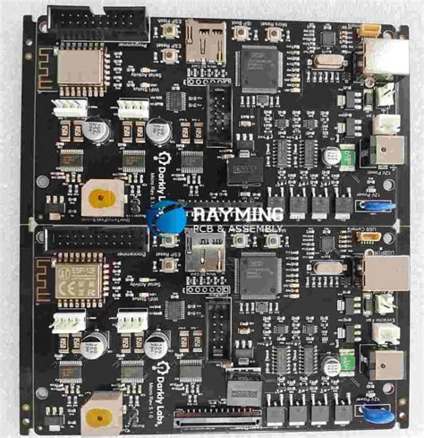
Advanced Strategies for Modern Surface Mount PCB Assembly

Key Takeaways
Modern PCB assembly processes demand meticulous attention to precision and scalability, particularly in surface mount technology (SMT) applications A critical starting point lies in solder paste application, where advancements in stencil design and jetting systems enable micron-level accuracy for high-density interconnects (HDIs) Optimizing this stage reduces defects like bridging or voids, directly impacting yield rates in PCBA production
Thermal management emerges as a cornerstone in dense layouts, where component proximity and power dissipation require advanced materials such as thermally conductive substrates or embedded heat sinks Engineers now leverage simulation tools to predict hotspots and optimize copper pour patterns, ensuring reliability in mission-critical applications
The integration of automated optical inspection (AOI) and X-ray systems has redefined quality assurance, enabling real-time detection of micro-scale defects These systems, combined with machine learning algorithms, achieve sub-10μm resolution, making them indispensable for miniaturized electronics
For component placement, strategies like split-vision alignment and adaptive pick-and-place algorithms address challenges in 01005-sized components and irregular geometries This is particularly vital for HDI boards, where via-in-pad and staggered micro-vias demand sub-millisecond positioning accuracy
As miniaturization pushes the boundaries of SMT assembly, manufacturers are adopting laser-direct imaging and low-temperature solder alloys to mitigate warpage in ultra-thin substrates Concurrently, advanced reflow soldering techniques—such as vacuum-assisted profiles—minimize void formation in ball grid arrays (BGAs)
Material innovation remains pivotal, especially for high-frequency PCBs, where low-Dk laminates and silver sintering pastes enhance signal integrity in 5G/mmWave applications Looking ahead, trends like 3D component stacking and AI-driven process optimization are poised to redefine surface mount PCB assembly, blending speed with nano-scale precision
By harmonizing these strategies, PCBA specialists can navigate the dual challenges of scaling production while maintaining six-sigma quality standards—a balance essential for next-generation electronics manufacturing

Precision Solder Paste Application Techniques
Achieving consistent solder paste deposition is foundational to reliable PCB assembly, particularly in high-density designs where sub-100µm pad spacing is common Modern PCBA workflows leverage stencil technology and advanced dispensing systems to optimize paste volume, shape, and alignment Electroformed nickel stencils, for instance, provide ±5µm aperture accuracy, enabling precise control over solder paste viscosity and void formation in micro-BGA and 01005 component applications
| Parameter | Optimal Range | Impact on Deposition |
|---|---|---|
| Stencil Thickness | 80–130µm | Determines paste volume |
| Squeegee Pressure | 03–06 kg/cm² | Affects aperture fill rates |
| Printing Speed | 10–50 mm/sec | Influences paste release |
"Stencil design remains the most overlooked variable in solder paste application A 10% reduction in aperture area can decrease bridging defects by 22% in ultra-fine-pitch assemblies." – IPC-7525D Guidelines
Automated optical alignment systems now compensate for substrate warpage and positional drift, achieving placement accuracies under 15µm For mixed-technology boards, step stencils enable variable paste heights across the PCB assembly, critical for hybrid designs combining 04mm-pitch QFNs with through-hole connectors Post-print inspection using 3D SPI (Solder Paste Inspection) systems identifies deviations as small as 5µm, flagging insufficient deposition or misalignment before reflow
Recent innovations include vacuum-assisted stenciling for low-clearance components and shear-thinning pastes that maintain consistency across temperature fluctuations These advancements address miniaturization challenges in PCBA, where even micron-level paste variations can cause opens or head-in-pillow defects
Key considerations:
- Solder paste alloys (SAC305 vs low-temperature variants) must align with component thermal limits
- Environmental controls (20–25°C, 40–60% RH) stabilize paste rheology during printing
- Stencil cleaning frequency should adapt to pad density – every 5–10 prints for boards with 500+ components
By integrating these strategies, manufacturers reduce rework rates by up to 38% while maintaining IPC Class 3 standards for aerospace and medical PCB assembly applications
Thermal Management in Dense PCB Layouts
Effective thermal management has become a cornerstone of modern PCB assembly, particularly as miniaturization pushes component density to unprecedented levels In high-density PCBA designs, heat accumulation can compromise signal integrity, accelerate component degradation, and even lead to catastrophic failures Engineers now prioritize thermal-aware layouts from the earliest design stages, integrating advanced strategies to balance performance and reliability
A critical approach involves optimizing copper pour configurations and thermal via placement to dissipate heat efficiently By strategically embedding thermal relief patterns beneath high-power components like BGAs or QFNs, designers create low-resistance pathways for heat transfer to inner layers or external heatsinks For PCBA projects requiring extreme miniaturization, materials with enhanced thermal conductivity—such as metal-core substrates or ceramic-filled laminates—are increasingly replacing traditional FR-4 in critical areas
Simulation tools play a pivotal role in predicting thermal hotspots before prototyping Computational fluid dynamics (CFD) models analyze airflow patterns in enclosures, while finite element analysis (FEA) maps temperature gradients across multilayer boards These insights guide the placement of thermal interface materials (TIMs) and passive cooling elements like heat spreaders In automotive or aerospace PCB assembly, where operating environments are harsh, designers often incorporate active cooling solutions such as microfluidic channels or thermoelectric coolers (TECs) alongside conventional methods
The interplay between solder joint reliability and thermal stress further complicates dense layouts Differential expansion rates between components and substrates during thermal cycling can fracture connections over time To mitigate this, reflow profiling must account for the thermal mass variations across the board, ensuring uniform heating during PCBA processes Additionally, underfill materials are applied to high-stress components like CSPs to distribute mechanical strain and enhance longevity
As 5G and IoT technologies demand faster signal propagation in compact formats, managing electromagnetic interference (EMI) alongside thermal loads has become a dual challenge Innovative shielding techniques, such as grounded copper fences or conformal coatings with thermal dissipation properties, address both concerns simultaneously These advancements underscore how modern PCB assembly techniques are evolving to meet the thermodynamic demands of next-generation electronics without sacrificing performance or footprint efficiency
Automated Inspection Systems for SMT Quality
Modern PCB assembly processes demand rigorous quality control to address the challenges of miniaturization and high-density interconnects (HDI) Automated inspection systems have become indispensable in PCBA production lines, ensuring defects like solder bridging, misaligned components, or insufficient solder joints are identified with micron-level accuracy Automated Optical Inspection (AOI) leverages high-resolution cameras and machine learning algorithms to scan solder paste deposition and component placement in real time, comparing results against digital twins of the design files For hidden defects under ball grid arrays (BGAs) or within multilayer boards, X-ray inspection (AXI) provides non-destructive internal imaging, critical for validating connections in advanced PCB assembly applications
The integration of statistical process control (SPC) software transforms inspection data into actionable insights, enabling engineers to fine-tune stencil designs or reflow profiles This closed-loop feedback is particularly vital when assembling boards with 01005-sized components or ultra-fine-pitch ICs, where even minor process deviations can lead to field failures Advanced systems now incorporate 3D solder paste inspection (SPI) to measure paste volume and height before component placement, preempting defects at the earliest stage of PCBA manufacturing
As component densities push the limits of thermal management and signal integrity, automated inspection adapts through multispectral analysis Infrared thermography maps heat distribution during functional testing, identifying hotspots that could compromise long-term reliability Meanwhile, automated electrical testing (AET) validates circuit continuity in high-frequency PCB assembly, ensuring impedance matching and minimizing signal loss
The shift toward Industry 40 has further enhanced these systems through IoT-enabled predictive maintenance and AI-driven anomaly detection By correlating inspection data with historical process parameters, manufacturers achieve zero-defect manufacturing targets while maintaining throughput speeds exceeding 50,000 components per hour—a necessity for automotive and aerospace-grade PCBA production
Component Placement Strategies for HDI Boards
Building upon precision solder paste application and thermal management principles, component placement strategies emerge as a pivotal factor in high-density interconnect (HDI) board manufacturing The shift toward miniaturized electronics demands meticulous planning to balance signal integrity, thermal performance, and mechanical stability For PCB assembly processes targeting HDI designs, engineers prioritize micro-component orientation and pad-to-pad spacing to mitigate electromagnetic interference (EMI) risks while accommodating shrinking form factors
A critical consideration involves optimizing placement algorithms for automated pick-and-place systems Modern PCBA workflows leverage machine vision with ±25μm accuracy to position 0201-sized components and finer-pitch ICs This precision minimizes solder bridging in tight layouts, particularly when working with via-in-pad structures common in HDI stacks To enhance reliability, designers adopt asymmetric pad geometries that improve solder joint formation during reflow, even with uneven thermal distribution across multilayer boards
Thermal management intersects directly with placement logic High-power components like FPGAs or RF modules require strategic positioning near thermal vias or embedded heat sinks However, crowding these elements risks creating localized hot spots that degrade adjacent passives Advanced PCB assembly software now integrates thermal simulation data to automate component spacing rules, dynamically adjusting layouts based on real-time heatmap projections
Signal integrity further complicates HDI placement strategies Designers employ angled component orientation (45° or 30°) to reduce trace lengths in high-speed circuits, a technique particularly effective in 5G and IoT PCBA applications Cross-talk prevention measures, such as shielding ground planes beneath BGA packages, are systematically mapped during placement planning
Emerging tools like 3D laser-laminated substrates introduce new variables, requiring adaptive placement protocols Manufacturers increasingly adopt mixed-technology workflows, combining surface-mount and embedded components within unified HDI architectures This approach demands revised design-for-manufacturing (DFM) guidelines, emphasizing sequential lamination compatibility and material expansion coefficients during placement planning
As HDI technology advances, the interplay between automated placement systems and intelligent DFM checks becomes indispensable By aligning component positioning with real-time process feedback, PCB assembly teams achieve sub-01% defect rates even in 18-layer HDI configurations—a critical benchmark for aerospace and medical electronics sectors pushing miniaturization boundaries

Miniaturization Challenges in SMT Assembly
The relentless drive toward smaller, denser electronics has made miniaturization a defining challenge in modern PCB assembly As component densities approach sub-millimeter scales, engineers face intricate trade-offs between functional performance, thermal stability, and manufacturing yield High-density interconnect (HDI) designs now routinely incorporate 01005-sized components and micro-BGAs, demanding unprecedented precision in PCBA processes
A critical bottleneck lies in component placement accuracy, where even micron-level deviations can cause bridging or open connections Advanced pick-and-place systems now leverage vision-aligned fiducial markers and real-time laser calibration to achieve placement tolerances below 30µm However, shrinking pad geometries exacerbate solder joint reliability issues, particularly under thermal cycling stress To mitigate this, assemblers are adopting Type 6/7 solder powders with finer particle distributions, enabling consistent paste deposition on 02mm pitch pads
Thermal management complexities intensify in miniaturized PCB assembly, as tightly packed components create localized heat islands Designers increasingly rely on embedded thermal vias and selective copper balancing to dissipate heat without compromising routing density Simultaneously, reflow profiling requires tighter control over ramp rates and peak temperatures to prevent warpage in ultra-thin substrates
The shift toward chip-scale packaging (CSP) and 3D-IC integrations further strains automated optical inspection (AOI) systems Traditional 2D inspection struggles with obscured joints in stacked configurations, pushing manufacturers to adopt 3D X-ray inspection and AI-driven defect recognition These tools not only improve fault detection but also provide predictive analytics for process optimization
While miniaturization unlocks innovations in wearables and IoT devices, it demands tighter collaboration between PCBA designers and process engineers Proactive design for manufacturability (DFM) reviews and virtual prototyping have become essential to balance electrical performance with assembly feasibility in this evolving landscape

Advanced Reflow Soldering Process Controls
The evolution of PCB assembly techniques has elevated reflow soldering from a basic thermal bonding process to a precision-driven phase in PCBA manufacturing Modern systems now integrate adaptive thermal profiling and closed-loop monitoring to address the challenges posed by high-density interconnects (HDIs) and mixed-component boards At the core of these advancements lies the ability to dynamically adjust temperature gradients across multiple zones, ensuring optimal solder joint formation while preventing thermal stress on sensitive components like micro-BGAs or ultra-thin resistors
Critical to this process is the implementation of real-time nitrogen inerting, which reduces oxidation risks during peak heating phases By maintaining oxygen levels below 50 ppm, manufacturers achieve smoother intermetallic compound (IMC) layers, directly enhancing PCB assembly reliability in aerospace and medical-grade applications Simultaneously, advanced flux activation algorithms synchronize with conveyor speed adjustments, compensating for variations in board thickness or component thermal mass
For PCBA professionals, the strategic use of predictive analytics has become indispensable Machine learning models trained on historical thermal data now forecast potential cold solder joints or tombstoning defects before they occur, enabling preemptive parameter tuning This data-driven approach is particularly vital when processing lead-free SAC305 alloys, where a narrow process window (±3°C) demands exact control over soak zones and time-above-liquidus (TAL)
The integration of multi-spectral thermal imaging further refines quality assurance, capturing microscopic variations in heat distribution across 01005-sized components This capability, combined with IoT-enabled oven networks, allows for centralized process optimization across multiple PCB assembly lines—a critical advantage for high-mix production environments As miniaturization trends push pad geometries below 150µm, these closed-loop thermal management systems ensure consistent results while reducing rework rates by up to 40% compared to conventional reflow methods
Material Selection for High-Frequency PCBs
The foundation of reliable PCB assembly in high-frequency applications lies in selecting substrates that balance electrical performance, thermal stability, and manufacturability For 5G communications, radar systems, and millimeter-wave devices, engineers prioritize materials with low dielectric constant (Dk) and ultra-low dissipation factor (Df) to minimize signal loss and phase distortion Advanced laminates like Rogers RO4000® series or PTFE-based substrates offer superior high-frequency characteristics compared to standard FR-4, though at a higher cost
Thermal management becomes critical when designing PCBA for high-power RF circuits Materials with high glass transition temperatures (Tg), such as Isola IS620 or Arlon 85N, maintain structural integrity during repeated thermal cycling in reflow soldering processes Copper-clad laminates with controlled coefficient of thermal expansion (CTE) prevent delamination in multi-layer boards, particularly when combining high-frequency layers with standard FR-4 cores for cost optimization
The rise of embedded passives in surface mount PCB assembly further complicates material choices Low-loss prepregs with precise dielectric thickness tolerances (±3%) enable consistent impedance control across HDI layouts For applications requiring extreme frequency stability, ceramic-filled PTFE composites like Taconic RF-35TC™ provide 1% Dk variation from -50°C to +150°C
Soldermask selection also impacts performance in high-frequency PCBA Liquid crystal polymer (LCP) coatings or modified epoxy resins with low moisture absorption rates (02%) prevent capacitance drift in humid environments When specifying surface finishes, electroless nickel immersion gold (ENIG) remains preferred for its flatness and oxidation resistance, though emerging alternatives like organic solderability preservatives (OSP) gain traction for ultra-high-speed digital circuits
As PCB assembly transitions to 77 GHz automotive radar and terahertz systems, material engineers now evaluate substrate roughness at the nanometer scale Smoother copper foils (Ra 03 µm) combined with low-profile treatments reduce skin effect losses, enabling 98% signal integrity retention across 24-layer automotive control modules These advancements underscore how strategic material selection bridges the gap between theoretical high-frequency performance and manufacturable PCBA solutions
Future Trends in Surface Mount PCB Technology
The evolution of surface mount PCB assembly is accelerating to meet demands for higher-density interconnects and energy-efficient manufacturing Emerging technologies like ultra-fine-pitch components (sub-03mm pitch) and embedded passive devices are redefining design paradigms, enabling PCBA solutions to achieve unprecedented miniaturization without compromising reliability Innovations in additive manufacturing are also gaining traction, with 3D-printed circuitry allowing for complex, multi-layer architectures that bypass traditional etching limitations
A critical shift lies in the integration of AI-driven process optimization Machine learning algorithms now analyze solder joint integrity in real-time during PCB assembly, predicting defects before they occur This aligns with the growing adoption of digital twin simulations, which virtualize PCBA workflows to refine thermal profiles and component placement strategies Such tools are indispensable for addressing signal integrity challenges in high-frequency designs, where materials like liquid crystal polymer (LCP) substrates are becoming essential for 5G and millimeter-wave applications
Sustainability is another transformative force Manufacturers are prioritizing lead-free solder alloys and low-temperature soldering techniques to reduce energy consumption and carbon footprints Concurrently, advancements in modular PCB designs enable easier component recycling—a response to tightening global e-waste regulations
Looking ahead, hybrid approaches combining surface mount technology with chip-on-board (CoB) methods will blur traditional boundaries, particularly in IoT and wearable electronics These systems demand heterogeneous integration of analog, digital, and RF components—a challenge requiring tighter collaboration between PCBA engineers and semiconductor developers As edge computing proliferates, the industry’s ability to balance thermal dissipation with component density will determine the next generation of PCB assembly breakthroughs
Conclusion
The evolution of surface mount PCB assembly reflects the electronics industry’s relentless pursuit of miniaturization, precision, and reliability As modern devices demand higher component density and enhanced performance, manufacturers must adopt advanced PCBA strategies that address thermal dissipation, material compatibility, and automated quality assurance Innovations in solder paste deposition and reflow profiling have become critical for maintaining joint integrity in high-density interconnects, while machine vision systems now play an indispensable role in detecting microscopic defects
A key takeaway is the growing interdependence between component placement accuracy and thermal dynamics in HDI boards Engineers are increasingly leveraging simulation tools to predict heat distribution and optimize layouts before production, reducing costly iterations Additionally, the shift toward high-frequency materials underscores the need for PCB assembly processes that minimize signal loss and impedance mismatches, particularly in 5G and IoT applications
Looking ahead, the integration of AI-driven analytics into SMT assembly lines will further refine process control, enabling real-time adjustments to solder paste viscosity, pick-and-place alignment, and oven temperature gradients These advancements not only enhance yield rates but also support the development of next-generation electronics requiring ultra-thin form factors and extreme environmental resilience
Ultimately, success in modern PCBA hinges on balancing technological innovation with operational pragmatism Manufacturers that prioritize continuous process optimization, workforce upskilling, and collaboration with material scientists will lead the charge in delivering smaller, faster, and more reliable electronic systems for tomorrow’s markets
Frequently Asked Questions
How does thermal management differ in modern high-density PCB assemblies?
Contemporary PCB assembly processes employ multilayer thermal vias and ceramic-filled substrates to dissipate heat in compact layouts Engineers prioritize PCBA designs with embedded copper planes and selective conformal coating to manage thermal stress in miniaturized components
What solder paste innovations improve precision in SMT applications?
Type 6/7 solder powders with particle sizes below 15µm enable finer stencil printing for 0201 components Advanced PCB assembly lines now integrate laser-cut stencils and real-time SPI (Solder Paste Inspection) systems to achieve ±10µm deposition accuracy, critical for high-frequency RF circuits
Why do automated inspection systems outperform manual checks in SMT?
AOI (Automated Optical Inspection) and 3D X-ray systems detect microscopic defects like head-in-pillow or tombstoning with 9998% accuracy These systems analyze 50,000+ joints/hour in PCBA production, ensuring compliance with IPC-A-610 Class 3 standards for aerospace and medical devices
How are component placement strategies evolving for HDI boards?
High-Density Interconnect (PCBA) designs require adaptive pick-and-place algorithms to handle 03mm pitch BGAs and 01005 passives Dual-lane feeders and vision-assisted robots now achieve placement speeds of 45,000 CPH (components per hour) with 15µm positional error
What material advancements address signal integrity in 5G PCB assemblies?
Low-Dk/Df laminates like Rogers 4350B and Isola Astra MT77 minimize dielectric losses above 28GHz PCB assembly workflows pair these with laser-drilled microvias to maintain impedance control in millimeter-wave antenna arrays
Optimize Your Next Project with Expert PCB Assembly
For tailored solutions in advanced surface mount technology, please click here to consult our PCBA engineering team Explore customized DFM analysis and prototyping services optimized for your high-density application requirements


