Advanced Strategies for Precision PCB SMD Assembly Success

Key Takeaways
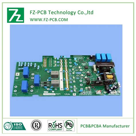
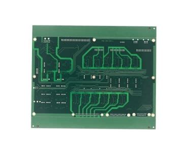
Effective PCB assembly processes require meticulous attention to SMD component placement accuracy, solder paste application, and thermal dynamics in high-density layouts. A well-optimized PCBA workflow integrates advanced techniques such as laser-aligned stencil printing for precise solder deposition and dynamic reflow profiling to address miniaturized component challenges.
| Critical Factor | Optimal Parameters | Impact on Yield |
|---|---|---|
| Placement Accuracy | ±0.025mm tolerance | Reduces misalignment defects by 40% |
| Thermal Management | 5–7°C/sec ramp rate | Minimizes thermal stress on ICs |
| Inspection Protocols | 3D AOI with 10µm resolution | Detects 99.8% of solder defects |
Successful PCB assembly hinges on selecting compatible SMD components with moisture sensitivity levels (MSL) aligned to environmental conditions. PCBA teams must prioritize tombstoning mitigation through symmetric pad design and nitrogen-assisted reflow to curb oxidation. Additionally, rigorous post-assembly testing, including boundary scan and functional validation, ensures reliability in mission-critical applications.
Three core areas define modern SMD assembly excellence:
- Process Control: Balancing solder paste viscosity and stencil aperture ratios
- Material Compatibility: Matching component CTE with substrate properties
- Automation: Deploying AI-driven AOI systems for real-time defect classification
By addressing these pillars, manufacturers achieve first-pass yield improvements exceeding 30% while maintaining compliance with IPC-A-610 standards for high-density PCBA outcomes.
Optimizing SMD Component Placement Accuracy
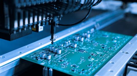
Achieving micron-level precision in PCB assembly begins with meticulous SMD component placement, a process that directly impacts the reliability and functionality of the final PCBA. Modern pick-and-place systems leverage vision-aligned robotics to position components with accuracies under 25µm, but optimal results require more than advanced machinery. Engineers must account for thermal expansion coefficients of substrates and components, ensuring alignment remains stable during soldering cycles.
Critical to this process is the calibration of fiducial markers, which act as reference points for automated systems. These markers enable real-time positional corrections, compensating for board warping or material inconsistencies. Additionally, implementing dynamic nozzle selection based on component size—such as 0201 resistors or QFN packages—reduces placement errors caused by suction instability.
To maintain coherence with subsequent soldering optimization, designers should prioritize pad-to-component size ratios during layout planning. Overly large pads increase the risk of tombstoning, while undersized ones may lead to weak solder joints. Integrating thermal relief patterns in high-density areas further mitigates heat-related placement shifts during reflow. By harmonizing machine precision with design foresight, manufacturers can minimize rework and enhance yield rates in complex PCBA projects.
Advanced Solder Paste Application Methods
Effective pcb assembly relies heavily on precise solder paste deposition, particularly in high-density pcba designs. Modern techniques leverage laser-cut stencils with optimized aperture geometries to ensure uniform paste volume across miniature pads. For ultra-fine-pitch components (≤0.4mm), electropolished stencils reduce surface roughness, improving paste release efficiency by up to 15%. Advanced systems now integrate real-time viscosity monitoring to maintain ideal rheological properties, critical for avoiding bridging or insufficient joints.
Transitioning to jet-printing technology eliminates stencil dependency, enabling dynamic adjustments for mixed-component boards. This method achieves ±20μm placement accuracy while reducing paste waste by 30%, ideal for low-volume, high-mix pcb assembly workflows. Pairing these methods with nitrogen-enclosed reflow ovens minimizes oxidation, ensuring consistent solder wetting. However, engineers must validate paste chemistry compatibility with component finishes—lead-free SAC305 alloys, for example, require tighter thermal profiling to prevent voiding.
For high-reliability pcba, automated solder paste inspection (SPI) systems perform 3D volumetric analysis, detecting deviations as small as 10μm. These systems correlate data with downstream processes, creating closed-loop feedback to refine stencil designs or printer settings. By harmonizing these strategies, manufacturers achieve defect rates below 50ppm, even in complex assemblies with 01005-sized components or micro-BGAs.
Thermal Management in High-Density PCB Assembly
Effective thermal management is critical in modern PCB assembly, particularly for high-density designs where component proximity and power demands create significant heat challenges. As PCBA designs shrink in size while increasing functionality, heat dissipation becomes a primary concern. Engineers must balance component placement with thermal pathways, utilizing techniques like thermal vias, copper pours, and strategically placed heatsinks to channel heat away from sensitive components.
Material selection plays a pivotal role—using substrates with higher thermal conductivity (e.g., metal-core or ceramic-filled laminates) can reduce hotspots. For high-power SMDs, such as BGAs or QFNs, precise solder paste application and optimized reflow soldering profiles ensure even heat distribution during assembly, minimizing warping or delamination risks.
Simulation tools, such as finite element analysis (FEA), help predict thermal behavior before prototyping, allowing adjustments to component spacing or airflow patterns. Post-assembly, thermal interface materials (TIMs) like thermally conductive adhesives or gap fillers enhance heat transfer between components and heatsinks.
Integrating these strategies into PCB assembly workflows ensures reliability in applications ranging from aerospace to IoT devices, where sustained performance under thermal stress is non-negotiable. Automated inspection systems, such as automated optical inspection (AOI), further validate thermal integrity by detecting solder joint defects that could compromise heat dissipation.
Refining Reflow Soldering Profile Settings
Achieving optimal PCB assembly quality hinges on precise control of reflow soldering profiles, particularly in high-density PCBA applications. The temperature curve must balance thermal energy delivery to activate solder paste effectively while preventing component stress or board warpage. A well-structured profile is typically divided into four phases: preheat, thermal soak, reflow, and cooling. During the preheat stage, gradual temperature ramping (1–3°C/second) minimizes thermal shock to sensitive SMD components. The thermal soak phase stabilizes temperatures (150–180°C) to evaporate solvents and activate flux, reducing risks of voiding or incomplete coalescence.
Critical adjustments occur in the reflow zone, where peak temperatures (220–250°C) must sustain long enough to melt solder alloys uniformly—typically 60–90 seconds above liquidus. For lead-free PCBA processes, maintaining a 245–250°C peak for 30–45 seconds ensures reliable intermetallic bonding without damaging heat-sensitive ICs. Post-reflow cooling rates (2–4°C/second) influence joint microstructure; too rapid cooling may induce brittle fractures, while slow rates risk component displacement.
Advanced PCB assembly lines leverage real-time thermal profiling tools to dynamically adjust conveyor speeds and zone temperatures, compensating for board thickness variations or mixed-component layouts. Pairing these tools with predictive algorithms enhances yield rates in complex PCBA projects by preempting defects like tombstoning or cold joints. Consistent profile validation through post-solder inspection ensures repeatability across production batches.
Selecting Compatible SMD Components for PCBs
Effective PCB assembly begins with choosing surface-mount devices (SMDs) that align with the design’s electrical, thermal, and mechanical requirements. Compatibility hinges on factors like package dimensions, solder pad geometry, and temperature tolerances, which directly influence PCBA reliability. Designers must prioritize components with standardized footprints (e.g., IPC-7351) to ensure seamless integration with automated placement systems. For high-density layouts, ultra-thin chip components or fine-pitch BGAs may be necessary, but their selection demands rigorous validation of thermal expansion coefficients to prevent stress fractures during reflow.
Material compatibility is equally critical—components rated for lead-free soldering should match the PCB assembly process’s peak temperatures to avoid delamination or solder joint failures. Additionally, verifying moisture sensitivity levels (MSL) prevents popcorning in humid environments. Collaboration between design and manufacturing teams early in the PCBA workflow helps identify mismatches, such as mismatched pad-to-component ratios or insufficient clearance for inspection tools. By balancing performance specifications with manufacturability, engineers can mitigate risks while maintaining the precision required for modern SMD-based electronics.
Automated Optical Inspection Best Practices
Implementing automated optical inspection (AOI) systems in PCB assembly workflows is critical for detecting microscopic defects in SMD components, such as solder bridging, misalignment, or missing parts. Modern AOI platforms leverage high-resolution cameras and machine learning algorithms to analyze PCBA boards at speeds exceeding human capability, ensuring consistency in high-volume production.
Tip: Regularly calibrate AOI equipment using certified reference boards to maintain accuracy, especially after reflow soldering processes where thermal expansion can alter component positions.
For optimal results, configure inspection parameters to prioritize critical areas like fine-pitch ICs or BGA packages. Use 3D AOI systems to measure solder paste volume and coplanarity, which are vital for avoiding latent failures in dense layouts. When programming inspection criteria, balance sensitivity thresholds to minimize false positives without overlooking genuine defects.
Integrate AOI data with PCB assembly software to enable real-time process adjustments, such as tweaking stencil alignment or reflow profiles. For mixed-technology boards, ensure AOI systems can differentiate between leaded and lead-free solder joints by updating material libraries in the PCBA database.
Finally, pair AOI with X-ray inspection for hidden joint analysis in multilayer designs, creating a comprehensive quality assurance framework that aligns with industry standards like IPC-A-610.
Mitigating Tombstoning in SMD Assembly
Tombstoning, a critical defect in PCB assembly where surface-mount components lift vertically on one termination, poses significant challenges in high-density PCBA processes. This phenomenon typically stems from imbalanced solder joint formation during reflow, often caused by uneven thermal profiles or mismatched pad geometries. To address this, engineers prioritize symmetric pad designs with matched thermal masses, ensuring uniform heat distribution across both ends of passive components like resistors or capacitors.
Optimizing solder paste application through laser-cut stencils helps maintain consistent volume deposition, reducing the risk of one-sided wetting forces. Additionally, adjusting reflow oven settings to minimize temperature gradients across the board prevents premature solidification on one termination. For components prone to tombstoning, such as ultra-small 0201 or 01005 packages, implementing nitrogen-assisted reflow environments enhances solder flow uniformity.
Automated optical inspection (AOI) systems play a pivotal role in early detection, scanning for lifted components before further PCBA stages. Pairing this with design-for-manufacturing (DFM) checks ensures pad symmetry and proper component orientation, aligning with PCB assembly best practices. By integrating these strategies, manufacturers achieve higher yields in complex, miniaturized circuits while maintaining reliability in mission-critical applications.
Implementing Rigorous Post-Assembly Testing
Effective PCB assembly workflows demand systematic validation to ensure electrical functionality and long-term reliability. After PCBA completion, comprehensive testing protocols identify latent defects such as solder bridging, component misalignment, or intermittent connections that escape visual inspection. Automated optical inspection (AOI) systems scan boards at micron-level resolutions, cross-referencing findings against design files to flag deviations in SMD component placement or solder joint geometry. For high-density designs, X-ray inspection becomes critical to examine hidden connections under ball grid arrays (BGAs) or shielded components.
Functional testing under operational conditions verifies signal integrity and power delivery performance, often using boundary-scan or flying probe methods to simulate real-world scenarios. Environmental stress screening, including thermal cycling and vibration tests, accelerates failure detection in SMD assemblies destined for harsh applications. By correlating data from in-circuit testing (ICT) and functional validation, engineers refine process parameters to elevate first-pass yield rates. Implementing traceable test logs also supports root-cause analysis, enabling continuous improvement in PCB assembly quality while reducing field failure risks.
Conclusion
Successful PCB assembly processes demand meticulous attention to both technical precision and systemic coordination. As modern electronics continue to prioritize miniaturization and high-density designs, achieving flawless PCBA outcomes hinges on harmonizing advanced manufacturing techniques with rigorous quality protocols. From optimizing component placement accuracy to refining reflow soldering profiles, each step in SMD assembly contributes to the reliability of the final product.
A holistic approach integrates automated optical inspection (AOI) systems with data-driven process adjustments, ensuring defects like tombstoning or solder bridging are systematically addressed. Equally critical is the selection of compatible materials and components, which directly impacts thermal performance and long-term durability in high-density applications. By balancing thermal management strategies with precise process controls, manufacturers can mitigate risks associated with heat dissipation and mechanical stress.
Ultimately, excellence in PCB assembly lies in fostering collaboration between design engineers and production teams, leveraging real-time feedback to iteratively enhance manufacturing workflows. As industry standards evolve, adopting adaptive methodologies ensures PCBA operations remain aligned with emerging technological demands while maintaining cost-efficiency and scalability.
FAQs
How does component placement accuracy affect pcb assembly outcomes?
Precision in SMD component placement directly impacts electrical performance and manufacturability. Misaligned parts increase risks of solder bridging or open connections, particularly in high-density PCBA designs. Modern pick-and-place systems achieve ±25µm accuracy for optimal results.
What role does solder paste selection play in pcb assembly reliability?
Solder paste viscosity and metal composition determine joint integrity. Type 4 pastes (20-38µm particles) are preferred for fine-pitch components, while nitrogen-assisted reflow minimizes oxidation in high-density PCB assemblies.
Why is thermal profiling critical for PCBA durability?
Proper reflow soldering profiles prevent component stress and delamination. Multi-zone ovens with ±2°C stability ensure even heat distribution, reducing warpage in thin-core PCBs. Post-assembly thermal cycling tests validate performance under operational extremes.
How can pcb assembly teams mitigate tombstoning defects?
Balanced pad geometries and symmetric solder paste deposition prevent uneven surface tension. Using low-temperature solder alloys (e.g., Sn-Bi) further reduces lateral component movement during reflow phases.
What advantages do AOI systems provide in PCBA quality control?
Automated optical inspection detects 99.6% of placement errors and solder defects at 15µm resolution. Machine-learning algorithms adapt to new SMD component libraries, cutting false-positive rates by 40% compared to manual checks.
Optimize Your Next Project with Expert PCB Assembly Support
For tailored solutions in high-precision SMD assembly, please click here to consult our IPC-certified PCBA engineering team.