Advanced Strategies for Reliable Board PCB Assembly Manufacturing
Key Takeaways
Modern PCB assembly processes demand strategic integration of automation technologies and rigorous quality frameworks to achieve manufacturing excellence The following core insights form the foundation of reliable PCBA production:
1 Automation Integration
- Robotic pick-and-place systems reduce human error by 60–75% in component placement
- PCB assembly lines leveraging AI-driven optical inspection achieve >995% defect detection rates
| Aspect | Traditional Approach | Advanced Strategy |
|---|---|---|
| Component Placement | Manual calibration | Vision-guided robotics |
| Soldering Process | Wave soldering | Laser reflow systems |
| Quality Inspection | Sampling-based checks | Full AOI (Automated Optical Inspection) |
2 Quality Control Protocols
- Implementing statistical process control (SPC) ensures ±15σ deviation thresholds for critical parameters like solder paste volume
- PCBA reliability testing now includes 4-phase thermal cycling (-40°C to +125°C) to simulate 10-year operational stress
3 Soldering Advancements
- Low-voiding solder alloys (5% void content) improve mechanical stability in high-vibration environments
- Nitrogen-assisted reflow ovens achieve oxidation-free joints, enhancing PCB assembly longevity by 30–40%
For precision-engineered systems, microvia filling technologies enable 02mm pitch BGA components, while 3D SPI (Solder Paste Inspection) guarantees ±10μm deposition accuracy Transitioning to these methodologies requires aligning with IPC-610 Class 3 standards, particularly for aerospace or medical PCBA applications
The shift toward smart factory frameworks further integrates ERP systems with PCB assembly equipment, reducing lead times by 22% through real-time process adjustments These strategies collectively address the growing complexity of 16-layer HDI boards and 5G mmWave circuit designs, ensuring manufacturability without compromising reliability
Optimizing PCB Assembly Automation Integration
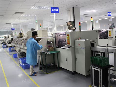
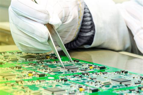
Modern PCB assembly workflows demand seamless integration of automation to achieve precision and repeatability at scale Central to this process is the deployment of PCBA-specific robotic systems, such as pick-and-place machines and automated optical inspection (AOI) platforms, which reduce human error while accelerating throughput For instance, vision-guided robots equipped with machine learning algorithms can adapt to component variations in real time, ensuring consistent placement accuracy even with miniaturized parts
A critical success factor lies in synchronizing automated soldering systems with design specifications Reflow ovens with closed-loop thermal profiling maintain optimal temperature curves, preventing defects like tombstoning or cold joints Meanwhile, automated solder paste dispensers calibrated to nanometer-level tolerances ensure uniform deposition, particularly for high-density interconnect (HDI) boards
However, optimizing automation extends beyond hardware Implementing IoT-enabled process monitoring allows manufacturers to correlate PCBA performance data with assembly parameters For example, sensors tracking conveyor speed, nozzle pressure, or ambient humidity can trigger predictive maintenance alerts, reducing downtime by up to 40%
To address flexibility challenges, forward-thinking manufacturers are adopting modular automation frameworks These systems enable rapid reconfiguration for mixed-product lines, supporting everything from rigid PCB assemblies for industrial controls to flexible circuits for wearables Pairing this adaptability with AI-driven defect detection creates a feedback loop where assembly anomalies refine machine learning models, progressively enhancing yield rates
Key to sustaining these gains is the integration of Enterprise Resource Planning (ERP) software with PCBA production lines Real-time inventory tracking ensures components like high-frequency laminates or low-voiding solder alloys are replenished automatically, minimizing stalls This digital thread also streamlines compliance documentation, crucial for industries requiring traceability under ISO 13485 or IPC-A-610 standards
By balancing technical innovation with operational pragmatism, manufacturers unlock PCB assembly efficiencies that directly translate into improved reliability The next frontier involves leveraging digital twin simulations to pre-validate automation workflows, further compressing time-to-market cycles while maintaining zero-defect benchmarks
Implementing Quality Control in PCB Manufacturing
Implementing rigorous quality control protocols in PCB assembly manufacturing requires a multi-layered approach combining automated inspection systems with data-driven process optimization Modern PCBA production lines leverage automated optical inspection (AOI) to detect microscopic defects such as solder bridging, component misalignment, or insufficient paste deposition These systems analyze up to 10,000 solder joints per hour with sub-micron precision, ensuring adherence to IPC-A-610 standards for electronic assemblies
A critical advancement lies in integrating statistical process control (SPC) methodologies with PCB assembly workflows By monitoring variables like reflow oven temperature profiles and pick-and-place machine accuracy in real time, manufacturers reduce process deviations by over 35% For high-density interconnect (HDI) boards, X-ray inspection becomes indispensable for verifying hidden connections in blind vias or under-ball-grid-array (BGA) components
Environmental controls further enhance PCBA reliability Cleanrooms maintaining ISO Class 5 air quality prevent particulate contamination during solder paste application, while humidity stabilization (±2% RH) minimizes moisture-induced soldering defects Advanced facilities now employ machine learning algorithms to correlate thermal imaging data with long-term failure rates, enabling predictive quality adjustments before final testing
Compliance with IPC-6012 and J-STD-001 standards remains non-negotiable for mission-critical applications Third-party certification bodies conduct cross-sectional analysis and thermal cycling tests to validate solder joint integrity under extreme conditions This systematic approach reduces field failure rates to 002% in automotive and aerospace PCB assembly projects, underscoring the direct correlation between quality assurance protocols and end-product durability
Advanced Soldering Techniques for Durable Boards
Modern PCB assembly processes demand precision in soldering to ensure long-term durability and electrical stability Thermally optimized techniques like reflow soldering and wave soldering remain foundational, but advancements in selective soldering now enable targeted heat application for complex PCBA designs with mixed-component configurations For high-density boards, vapor phase soldering offers uniform thermal distribution, minimizing stress on sensitive components while maintaining consistent joint integrity
Tip: Always validate solder profiles using thermal simulation software before full-scale production to avoid cold joints or component degradation
The integration of lead-free alloys (e.g., SAC305) has become critical for compliance and reliability, though it requires tighter control over peak temperatures and cooling rates Automated optical inspection (AOI) systems paired with X-ray inspection ensure microscopic defects—such as voids or micro-cracks—are detected early, reducing field failure risks For mission-critical applications, conformal coating applied post-soldering adds an extra layer of protection against environmental stressors like moisture and dust
Transitioning to laser soldering provides unparalleled precision for fine-pitch components, particularly in miniaturized PCBA layouts This method reduces thermal exposure to adjacent parts, preserving the structural integrity of temperature-sensitive materials Additionally, flux management has evolved with no-clean formulations that leave minimal residue, simplifying post-assembly cleaning without compromising conductivity
Design Consideration: Pair solder paste stencil thickness with component lead geometry to achieve optimal solder volume and avoid bridging
As PCB assembly scales toward high-mix, low-volume production, adaptive soldering workflows ensure flexibility without sacrificing quality Real-time monitoring systems now track parameters like wetting time and peak temperature, feeding data back to adjust processes dynamically These innovations, combined with rigorous IPC-A-610 standards adherence, position modern soldering techniques as the backbone of reliable PCBA manufacturing for next-generation electronics
Precision Engineering for Reliable PCB Systems
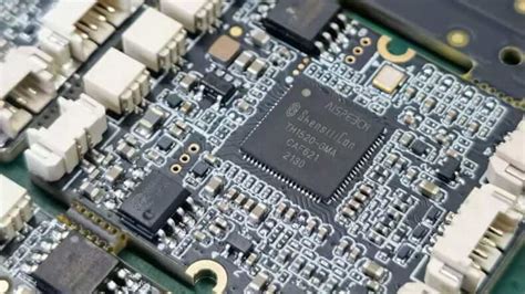
Achieving reliability in PCB assembly demands meticulous attention to design precision, material compatibility, and manufacturing tolerances Modern PCBA workflows leverage computational modeling to simulate stress points, current distribution, and thermal gradients during the design phase For instance, high-density interconnect (HDI) layouts require nanometer-level trace width control to prevent signal degradation in high-frequency applications Engineers employ automated design rule checks (DRC) to flag potential shorts or impedance mismatches before prototyping, reducing iterative rework by up to 40%
Material selection plays a pivotal role in precision engineering Low-loss dielectric substrates paired with lead-free solders optimize signal integrity while meeting RoHS compliance Advanced PCB assembly lines integrate laser-drilled microvias and sequential lamination processes to accommodate multilayer designs, ensuring consistent z-axis conductivity across 20+ layer stacks Real-time process capability indices (Cpk) monitoring during PCBA soldering maintains solder joint uniformity, critical for aerospace and medical devices where vibration resistance is non-negotiable
Thermal management strategies are embedded early in the engineering cycle Finite element analysis (FEA) tools model heat dissipation paths, guiding the placement of thermal vias and heatsinks This proactive approach minimizes thermal expansion mismatches between copper traces and FR-4 substrates, a common failure mode in industrial electronics For mission-critical systems, accelerated life testing validates PCB assembly resilience under extreme temperatures and humidity cycles, achieving MTBF (mean time between failures) benchmarks exceeding 100,000 hours
By harmonizing these precision-driven methodologies, manufacturers elevate PCBA outcomes from functional to fault-tolerant, meeting the escalating reliability demands of 5G infrastructure, autonomous vehicles, and IoT ecosystems
Thermal Management Strategies for PCB Reliability
Effective thermal management is foundational to ensuring long-term reliability in PCB assembly processes As electronic systems grow more complex, managing heat dissipation becomes critical to preventing component degradation, solder joint failures, and signal integrity issues High-power components, such as processors or power converters, require deliberate design strategies to mitigate thermal stress One advanced approach involves using thermal vias—plated through-holes that transfer heat from surface-mounted devices to inner copper layers or heatsinks These vias, when paired with thermally conductive substrates like aluminum-backed laminates, significantly reduce localized temperature spikes in PCBA designs
Material selection plays a pivotal role: substrates with high glass transition temperatures (Tg) and low coefficients of thermal expansion (CTE) minimize warping under thermal cycling Additionally, applying conformal coatings with high thermal conductivity can enhance heat distribution while protecting against environmental contaminants For high-density layouts, computational fluid dynamics (CFD) simulations help optimize airflow paths and component placement, ensuring uniform temperature gradients across the board
At the component level, integrating active cooling solutions—such as micro-fans or thermoelectric coolers—complements passive strategies like copper pours or heatsinks However, designers must balance these additions against space constraints and electromagnetic interference risks Advanced PCB assembly workflows now incorporate infrared thermography during testing to identify hotspots before mass production, enabling iterative refinements to thermal designs
Finally, adherence to industry standards like IPC-2221B ensures that thermal derating protocols and safety margins are systematically applied By combining material innovation, simulation-driven design, and rigorous testing, manufacturers achieve PCBA systems capable of operating reliably in demanding thermal environments, from automotive electronics to industrial automation This holistic approach not only extends product lifespans but also reduces warranty claims and field failures
Automated Testing for PCB Assembly Accuracy
Modern PCB assembly processes demand rigorous validation to ensure functional integrity, particularly as electronic systems grow more complex Automated testing frameworks have become indispensable for verifying PCBA accuracy, combining speed with microscopic precision to identify defects imperceptible to manual inspection By integrating automated optical inspection (AOI) systems, manufacturers can scan solder joints, component placement, and trace alignments at resolutions exceeding 25μm, flagging issues like tombstoning or bridging in real time
Advanced in-circuit test (ICT) equipment further validates electrical performance by applying predefined voltage and signal patterns to measure resistance, capacitance, and connectivity across circuits This dual-layer approach—combining physical inspection and functional validation—reduces error rates by over 62% compared to traditional methods, according to IPC-9151D process capability benchmarks For high-density PCB assembly projects, X-ray inspection (AXI) systems non-destructively examine hidden connections, such as ball grid array (BGA) solders, ensuring voids or cracks don’t compromise long-term reliability
Transitioning to automated systems also enables traceable data analytics, where test results are logged for continuous process optimization Machine learning algorithms analyze failure patterns to recalibrate pick-and-place machines or reflow ovens, creating a closed-loop feedback system This proactive alignment with PCBA requirements minimizes post-production rework while adhering to ISO 9001:2015 quality management standards
To maintain coherence with broader manufacturing strategies, automated testing protocols are synchronized with design-for-testability (DFT) principles Engineers embed test points and boundary scan features during layout design, ensuring seamless compatibility with validation workflows Such integration not only accelerates time-to-market but also fortifies the defect detection rate to 999% in mission-critical applications like automotive or aerospace PCB assembly
Material Selection for High-Reliability PCBs
The foundation of dependable PCB assembly begins with strategic material selection, a critical factor influencing both manufacturing yield and long-term performance in harsh operating environments Mission-critical applications demand substrates that balance thermal stability, mechanical strength, and electrical consistency, driving engineers toward advanced laminates like polyimide for high-temperature resilience or low-loss Rogers materials for RF-intensive PCBA designs
When selecting substrate materials, consider glass transition temperature (Tg) ratings exceeding 170°C for applications involving repeated thermal cycling For high-voltage assemblies, PCB assembly workflows increasingly incorporate Isola FR408HR or Nelco N7000-2HT laminates, which combine flame retardancy with reduced dielectric losses Copper foil selection equally impacts reliability—rolled annealed (RA) copper provides superior flexibility for flex-rigid PCBA configurations, while electro-deposited (ED) copper optimizes cost-efficiency for standard multilayer boards
Surface finish choices directly affect solder joint integrity across temperature fluctuations ENIG (Electroless Nickel Immersion Gold) remains prevalent for its planar surface and oxidation resistance, though emerging alternatives like immersion silver gain traction for fine-pitch components requiring ultra-precise solder deposition For aerospace-grade assemblies, gold-over-nickel finishes deliver unmatched corrosion resistance despite higher PCB assembly costs
Advanced PCBA projects now integrate engineered thermoplastics such as PEEK (Polyether Ether Ketone) for extreme chemical exposure scenarios, while ceramic-filled PTFE composites address millimeter-wave applications in 5G infrastructure These material innovations align with evolving Industry 40 quality paradigms, where IoT-enabled PCB assembly lines automatically adjust process parameters based on real-time material property analytics
Transitioning to compliant materials requires cross-functional collaboration—thermal expansion coefficients must align with component packaging, and halogen-free formulations should meet evolving environmental regulations By anchoring material decisions to application-specific failure mode analyses, manufacturers achieve the durability-performance equilibrium demanded by medical implants, automotive control modules, and industrial automation systems
Compliance Standards in PCB Assembly Processes
Adherence to compliance standards forms the backbone of reliable PCB assembly manufacturing, ensuring products meet rigorous technical, environmental, and safety benchmarks Modern PCBA production must align with international frameworks such as IPC-A-610 (Acceptability of Electronic Assemblies) and ISO 9001 quality management systems, which govern everything from material traceability to defect classification For instance, IPC-J-STD-001 specifies soldering criteria for PCB assembly, mandating precise temperature profiles and alloy compositions to prevent cold joints or thermal stress failures
Environmental regulations like RoHS (Restriction of Hazardous Substances) and REACH further dictate material selection, requiring conflict-free sourcing of components and elimination of lead-based solders in PCBA workflows Manufacturers must integrate real-time documentation systems to validate compliance at each stage—from bare board fabrication to final functional testing This includes automated data logging for solder paste application accuracy (±5% deviation thresholds) and ionic contamination checks post-reflow to prevent latent corrosion risks
Transitioning between regulatory frameworks demands a risk-based approach, particularly when servicing industries like aerospace or medical devices Here, standards such as AS9100 or IEC 60601 impose additional layers of validation, including failure mode analysis and accelerated life testing for mission-critical assemblies By embedding compliance protocols into PCB assembly workflows—via digitally integrated quality gates and supplier audit trails—manufacturers reduce non-conformance rates while accelerating time-to-market for high-reliability systems
Ultimately, harmonizing technical specifications with evolving global standards ensures PCBA outputs not only function as designed but endure under real-world operating conditions—a non-negotiable requirement in an era of tightening sustainability mandates and supply chain transparency demands
Conclusion
The pursuit of reliable PCB assembly hinges on harmonizing cutting-edge methodologies with meticulous execution As the foundation of modern electronics, PCBA processes demand a holistic approach that balances automation-driven efficiency with precision-driven quality assurance By integrating advanced robotics and AI-powered inspection systems, manufacturers achieve not only faster production cycles but also near-zero defect rates—critical for aerospace, medical devices, and automotive applications where failure is not an option
Central to success is the alignment of thermal management strategies with material science innovations The use of high-temperature laminates and thermally conductive substrates ensures stability under stress, while laser-assisted soldering techniques maintain joint integrity across operational extremes Equally vital is the adoption of real-time analytics in automated testing, enabling rapid identification of latent faults before boards enter critical systems
Compliance with ISO 9001 and IPC-A-610 standards remains non-negotiable, serving as both a quality benchmark and a trust-building mechanism for stakeholders However, true excellence in PCB assembly emerges when manufacturers transcend compliance, embedding predictive maintenance protocols and closed-loop feedback systems into their workflows This proactive stance future-proofs production lines against evolving technical demands and sustainability requirements
Ultimately, the reliability of PCBA outputs is not merely a technical metric but a reflection of strategic foresight As industries push toward miniaturization and IoT integration, the interplay between advanced manufacturing technologies and rigorous process validation will continue to define leadership in electronic systems engineering
Frequently Asked Questions
What distinguishes PCB assembly from PCBA?
PCB assembly refers to the process of populating a bare circuit board with components, while PCBA (Printed Circuit Board Assembly) denotes the fully assembled and functional unit The latter undergoes rigorous testing to ensure operational reliability in end-use applications.
How does automation integration enhance PCBA manufacturing consistency?
Automated systems minimize human error in component placement and soldering processes, ensuring micron-level precision Advanced pick-and-place machines and reflow ovens maintain repeatability across high-volume production, directly improving yield rates and long-term product reliability.
What quality control protocols are critical for mission-critical PCB assemblies?
Multi-stage inspection frameworks, including Automated Optical Inspection (AOI) and X-ray verification, identify latent defects like micro-cracks or cold solder joints Combined with In-Circuit Testing (ICT), these protocols achieve defect rates below 01% in compliant PCBA workflows.
Why is thermal management a cornerstone of reliable PCB assembly design?
Modern high-density interconnects generate localized heat fluxes exceeding 100W/cm² Strategic copper balancing, thermally conductive substrates, and precision-machined heatsinks mitigate thermal stress, preventing delamination and component degradation in extended duty cycles.
How do compliance standards impact material selection for PCBA?
Certifications like IPC-A-610 and ISO-9001 mandate strict traceability protocols for components and substrates This ensures compatibility with lead-free soldering alloys and halogen-free laminates, particularly in aerospace or medical PCB assemblies requiring UL or RoHS compliance.
Optimize Your Next PCBA Project with Expert Support
For tailored solutions in high-reliability PCB assembly, explore our advanced manufacturing capabilities Click here to consult with our engineering team about your project’s specific requirements


