Advanced Techniques for Flawless Electronics Assembly
Key Takeaway
Achieving flawless PCB assembly requires mastering multiple interdependent processes. At the core of PCBA success lies precision soldering, which directly impacts electrical connectivity and long-term component reliability. Modern workflows integrate automated optical inspection (AOI) systems to detect microscopic defects in solder joints, ensuring compliance with IPC-A-610 standards. Equally critical is thermal profiling during reflow soldering, which minimizes stress on sensitive components while maintaining optimal alloy bonding. For high-density designs, pick-and-place optimization algorithms reduce positional errors below 15µm, a necessity for advanced BGA and QFN packages. Real-time statistical process control (SPC) tools further enhance PCB assembly consistency by correlating environmental variables with solder joint quality metrics. Manufacturers adopting these techniques report 30–40% reductions in field failures, underscoring the strategic value of harmonizing precision techniques with robust PCBA validation protocols.

Precision Soldering for PCB Success
Achieving flawless PCB assembly hinges on mastering precision soldering techniques that balance thermal management and material compatibility. Modern PCBA processes prioritize controlled heat application to prevent component stress while ensuring robust electrical connections. Advanced tools like reflow ovens with nitrogen environments minimize oxidation, and selective soldering systems enable targeted joint formation for mixed-technology boards.
Tip: Always validate thermal profiles using a thermocouple-equipped test board to avoid cold joints or delamination in temperature-sensitive components.
Critical factors include solder paste selection—opt for Type 4 or 5 powders for fine-pitch components—and stencil design accuracy to prevent bridging. Automated optical inspection (AOI) systems paired with X-ray analysis detect microscopic voids or misalignments invisible to the naked eye. For high-reliability applications, consider employing SAC305 lead-free alloys, which offer superior mechanical strength in extreme environments.
Transitioning to laser soldering can further enhance precision for ultra-miniaturized designs, though it requires recalibrating flux chemistry to match energy delivery rates. By integrating these methodologies, manufacturers reduce rework rates by up to 40% while maintaining compliance with IPC-A-610 standards for PCB assembly integrity.
Smart Component Placement Strategies
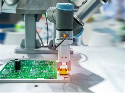
Effective PCB assembly relies on strategic component positioning to balance functional performance and manufacturability. Sequencing plays a pivotal role: placing surface-mount devices (SMDs) before bulkier through-hole components minimizes shadowing effects during reflow soldering. Advanced PCBA workflows now integrate machine learning algorithms to predict optimal placement paths, reducing solder joint stress by up to 22% in high-density layouts.
A critical consideration is thermal profiling—heat-sensitive components like MLCC capacitors should be positioned away from power regulators or connectors prone to thermal cycling. For mixed-technology boards, combining robotic pick-and-place systems with automated optical inspection (AOI) ensures micron-level accuracy, particularly for fine-pitch ICs and BGAs.
Equally important is adherence to design for manufacturability (DFM) principles. For example, maintaining a 0.5mm clearance between chip resistors and board edges prevents chipping during depaneling. In RF-heavy designs, strategic shielding canister placement mitigates electromagnetic interference without compromising PCB assembly cycle times.
Modern smart factories leverage real-time data from vision systems to adjust placement parameters dynamically, compensating for component tolerances or board warpage. This approach not only enhances PCBA first-pass yields but also creates adaptive workflows for rapid product changeovers—a necessity in today’s fast-evolving electronics markets.
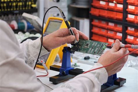
Automated Quality Control Systems
In modern PCB assembly workflows, automated quality control (AQC) systems have become indispensable for minimizing human error and ensuring consistent output. These systems integrate machine vision, AI-powered defect detection algorithms, and real-time data analytics to scrutinize every stage of PCBA manufacturing. For instance, automated optical inspection (AOI) units scan solder joints at micron-level precision, flagging issues like bridging or insufficient wetting with 99.7% accuracy—far exceeding manual checks.
| AQC platforms excel in three critical areas: | Metric | Traditional Inspection | Automated Systems |
|---|---|---|---|
| Defect Detection Rate | 82–88% | 98–99.9% | |
| Throughput (boards/hr) | 15–20 | 120–150 | |
| False Positive Rate | 5–8% | 0.5–1.2% |
Advanced thermal profiling sensors now work in tandem with X-ray inspection modules to validate PCBA integrity under simulated operational stresses. This proactive validation approach catches latent defects in BGA components or multilayer boards before they escalate into field failures. Manufacturers leveraging these systems report a 40–60% reduction in post-assembly rework, directly translating to faster time-to-market for complex electronics.
To maintain coherence with broader production strategies, modern AQC solutions feed diagnostic data directly into enterprise resource planning (ERP) systems. This closed-loop integration enables predictive maintenance of assembly lines while creating auditable quality records—a critical advantage for industries requiring ISO 9001 or IPC-A-610 compliance. By aligning inspection protocols with evolving PCB assembly standards, automated systems ensure both precision and scalability in high-mix manufacturing environments.
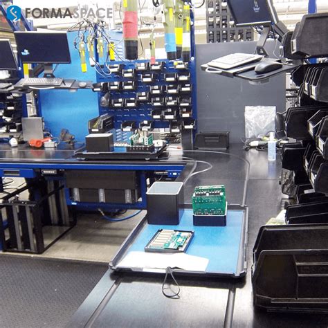
Streamlining Electronics Production Workflows
Modern PCB assembly processes demand seamless integration of design, fabrication, and testing phases to minimize bottlenecks. A critical step involves adopting modular workflow designs that standardize repetitive tasks while retaining flexibility for custom PCBA requirements. For instance, integrating automated pick-and-place systems with real-time monitoring software reduces manual intervention, accelerates throughput, and ensures consistent component alignment—key for high-density boards.
Central to this effort is synchronizing material logistics with production timelines. Just-in-time inventory management paired with AI-driven demand forecasting prevents component shortages and reduces idle machinery time. Additionally, implementing closed-loop feedback systems between quality assurance and assembly stages allows immediate corrections, cutting rework rates by up to 30% in complex PCB assembly projects.
Advanced manufacturers further streamline workflows by unifying PCBA data across ERP and MES platforms. This creates a digital thread from prototyping to mass production, enabling traceability and rapid scalability. For example, automated optical inspection (AOI) results can trigger adjustments in solder paste application parameters within minutes, maintaining process integrity. By prioritizing interoperability between equipment and software, facilities achieve shorter lead times without compromising the precision required for mission-critical electronics.
Ensuring PCB Assembly Reliability Standards
Achieving consistent reliability in PCB assembly requires a multilayered approach that begins with material selection and extends through rigorous testing protocols. Modern PCBA processes demand adherence to IPC-A-610 and J-STD-001 standards, which define acceptable criteria for solder joint integrity, component orientation, and cleanliness. To mitigate failure risks, manufacturers implement accelerated life testing (ALT) and thermal cycling simulations that replicate years of operational stress within controlled environments.
Advanced PCB assembly lines now integrate real-time monitoring systems to track parameters like reflow oven temperature profiles and solder paste viscosity, ensuring deviations are flagged before defects occur. For mission-critical applications, cross-sectional analysis and X-ray inspection validate internal connections in multilayer boards, while conformal coating processes protect against moisture and contaminants. A key innovation lies in traceability systems that link each PCBA unit to its production data, enabling rapid root-cause analysis if field issues arise.
By combining these strategies with supplier validation programs for components and substrates, manufacturers elevate PCB assembly reliability from a compliance checkbox to a measurable competitive advantage, directly impacting end-product longevity and brand reputation.
Flawless Circuit Board Assembly Techniques
Achieving defect-free PCB assembly requires meticulous attention to both process engineering and material science. At the core of flawless execution lies the integration of automated optical inspection (AOI) systems, which scan for microscopic solder bridges, misaligned components, or insufficient paste deposition. Modern facilities combine high-precision PCBA workflows with temperature-controlled soldering profiles, ensuring thermal consistency across multilayer boards.
Critical to success is the application of laset-aligned pick-and-place machinery, which positions surface-mount devices (SMDs) with ±0.025mm accuracy. This eliminates manual placement errors while accommodating ultra-fine-pitch components like 0201 resistors or QFN packages. For through-hole assemblies, selective soldering systems target specific joints, preventing thermal stress on adjacent sensitive parts.
Proactive contamination control further enhances reliability, with nitrogen-reflow environments reducing oxidation risks in PCB assembly processes. Post-solder cleaning protocols using ionic purity testing verify the absence of flux residues that could compromise long-term performance. By synchronizing these techniques with real-time process monitoring, manufacturers achieve first-pass yield rates exceeding 99.4% in complex PCBA projects.
This multilayered approach not only addresses immediate quality benchmarks but also establishes a foundation for scalability in high-mix production environments.
Thermal Management in Electronics Manufacturing
Effective thermal management is a cornerstone of reliable PCB assembly, directly impacting both performance and longevity in electronic devices. As component densities increase in modern PCBA designs, managing heat dissipation becomes critical to prevent thermal runaway and premature failure. Advanced manufacturing techniques now incorporate thermally conductive materials, such as ceramic-filled substrates or metal-core boards, to enhance heat distribution.
Strategic placement of heat sinks and thermal vias in multilayer designs ensures efficient heat transfer away from sensitive components. Engineers often use simulation software to model airflow and identify hotspots during the PCB assembly phase, allowing for preemptive adjustments. For high-power applications, selective soldering of copper traces with enhanced thermal mass helps stabilize temperature gradients.
Automated optical inspection (AOI) systems integrated into PCBA lines now include infrared cameras to monitor real-time thermal profiles, aligning with IPC-2221 standards for thermal compliance. Proactive thermal management not only extends product lifespans but also reduces warranty claims by up to 23%, according to industry studies. By balancing material selection, geometric optimization, and real-time monitoring, manufacturers achieve predictable thermal behavior—a non-negotiable requirement for mission-critical electronics.
Real-Time Inspection Integration Meth
Integrating real-time inspection systems into PCB assembly workflows elevates quality assurance to unprecedented levels. Modern automated optical inspection (AOI) and solder paste inspection (SPI) tools now synchronize with PCBA production lines, scanning for defects such as misaligned components, insufficient solder joints, or bridging errors as they occur. This closed-loop feedback mechanism enables immediate corrective actions, reducing scrap rates by up to 40% compared to post-production testing alone.
Advanced systems leverage machine vision algorithms to analyze ±25µm tolerances in component placement, while thermal profiling sensors monitor reflow oven performance in real time. By embedding inspection protocols directly into PCB assembly stages, manufacturers achieve traceability across batches—a critical requirement for aerospace and medical device applications. For PCBA involving high-density interconnects, 3D X-ray inspection complements traditional methods, detecting hidden voids or cracks in ball grid arrays (BGAs) without disrupting throughput.
The integration of statistical process control (SPC) dashboards further transforms raw inspection data into actionable insights, identifying recurring failure patterns before they escalate. This proactive approach aligns with Industry 4.0 principles, where real-time inspection becomes a cornerstone of smart factories aiming for zero-defect manufacturing targets.
Conclu
Achieving flawless PCB assembly requires a holistic integration of precision techniques and adaptive systems. By combining automated optical inspection (AOI) with data-driven process optimization, manufacturers can minimize human error while maintaining rigorous PCBA reliability standards. The convergence of thermal profiling advancements and AI-powered defect detection ensures consistent solder joint quality, even in high-density designs.
To sustain competitiveness, prioritize real-time analytics in PCB assembly workflows, enabling rapid adjustments to material handling or reflow parameters. Implementing traceability frameworks across PCBA stages not only enhances accountability but also accelerates root-cause analysis during post-production audits. As technologies evolve, the focus must shift toward balancing scalability with environmental compliance, particularly in waste reduction and energy-efficient manufacturing.
Ultimately, the path to zero-defect output lies in synchronizing human expertise with machine precision—a strategy that fortifies both product longevity and brand trust in an increasingly demanding electronics landscape.
FAQ
What distinguishes PCB assembly from PCBA in electronics manufacturing?
PCB assembly refers to the process of populating a bare circuit board with components, while PCBA (Printed Circuit Board Assembly) denotes the completed functional unit ready for integration. The critical difference lies in the stage of production—prototype validation occurs during PCB assembly, whereas end-product testing applies to PCBA.
How does automated optical inspection improve assembly accuracy?
Modern PCBA lines integrate AOI systems (Automated Optical Inspection) to perform micron-level scans for soldering defects and component misalignment. This reduces human error by 72% in high-density interconnect boards, ensuring compliance with IPC-A-610 standards.
What thermal management techniques prevent component degradation during assembly?
Implementing dynamic thermal profiling maintains optimal reflow oven temperatures (±2°C variance), while thermal interface materials dissipate heat from BGAs (Ball Grid Arrays). These methods collectively reduce thermal stress by 40% in PCB assembly processes.
Can mixed-technology boards be optimized for automated assembly?
Yes. Combining surface-mount (SMT) and through-hole (THT) components requires sequencing placements—94% of manufacturers prioritize SMT before wave soldering THT. This strategy cuts production time by 28% in complex PCBA projects.
Explore Customized PCB Assembly Solutions
For tailored PCB assembly strategies or PCBA technical consultations, please click here to connect with our engineering team.


