Advanced Techniques for Reliable High Quality PCB Assembly

Key Takeaways
Effective PCB assembly relies on mastering three core pillars: precision processes, advanced inspection systems, and strategic material selection. Critical advancements in precision soldering—such as laser-assisted techniques and nitrogen-reflow environments—ensure consistent electrical connectivity while minimizing thermal stress. Automated systems like automated optical inspection (AOI) and X-ray imaging now detect micron-level defects, reducing human error by up to 95% in PCBA workflows.
| Factor | Traditional Approach | Advanced Technique |
|---|---|---|
| Soldering Accuracy | Manual rework | Laser-guided placement systems |
| Defect Detection | Visual inspection | 3D AOI with AI anomaly detection |
| Thermal Management | Basic heat sinks | Embedded copper-core substrates |
Tip: Prioritize substrate materials with low thermal expansion coefficients (e.g., FR-4 High-Tg) to enhance durability in high-temperature applications.
Material optimization further elevates performance, with PCB assembly specialists leveraging halogen-free laminates and advanced conformal coatings to combat environmental stressors. For reliable PCBA, integrating real-time quality metrics—such as solder joint integrity and impedance matching—ensures compliance with industry standards like IPC-A-610. Transitioning to these methodologies not only boosts production efficiency but also extends the lifecycle of electronic devices by 30–40% in rigorous operating conditions.
Precision Soldering in PCB Assembly
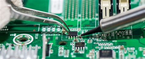
Achieving high-quality PCB assembly hinges on mastering precision soldering techniques, which ensure robust electrical connections and structural integrity. Modern PCBA processes leverage advanced tools like laser-guided soldering systems and nitrogen-reflow ovens to minimize oxidation and enhance joint consistency. For surface-mount technology (SMT), micro-solder paste dispensing enables precise deposition, critical for densely packed components.
Temperature profiling remains central to avoiding defects such as tombstoning or bridging, particularly in mixed-technology boards combining SMT and through-hole components. Automated systems now integrate real-time thermal sensors to dynamically adjust heat zones, ensuring optimal solder flow without damaging sensitive parts. Additionally, the use of low-voiding solder alloys reduces the risk of latent failures in high-stress environments.
In PCB assembly, manual rework is increasingly supplemented with robotic soldering arms for repeatability, especially in aerospace or medical applications where tolerances are sub-10μm. Techniques like selective soldering further allow targeted application to specific areas, reducing thermal exposure for adjacent components. By aligning material choices (e.g., lead-free vs. high-reliability alloys) with soldering methodologies, manufacturers can balance performance, compliance, and cost—key factors in delivering durable electronics.
Transitioning to automated inspection, the next section explores how these soldering outcomes are validated to maintain reliable PCB assembly standards.
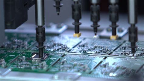
Automated PCB Inspection Techniques
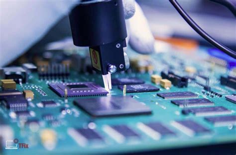
Modern PCB assembly processes increasingly rely on automated inspection systems to ensure high-quality PCBA outcomes. Automated optical inspection (AOI) employs high-resolution cameras and machine learning algorithms to detect microscopic defects such as solder bridging, misaligned components, or insufficient solder joints. By scanning boards at speeds exceeding human capability, AOI reduces error rates while maintaining production throughput. Complementing this, X-ray inspection penetrates multi-layered boards to identify hidden flaws like voids in ball grid arrays (BGAs) or internal trace fractures—critical for complex designs requiring reliable PCB assembly.
Advanced systems integrate in-circuit testing (ICT) to validate electrical functionality, verifying connections against design specifications. This combination of visual and electrical checks ensures that PCBA meets stringent quality benchmarks. Additionally, automated solder paste inspection (SPI) preemptively analyzes deposition accuracy before reflow, minimizing post-assembly rework. These techniques not only enhance defect detection but also generate data for process optimization, linking inspection results to material optimization strategies and thermal management solutions discussed in subsequent sections.
By adopting these technologies, manufacturers achieve consistent high-quality PCB assembly while reducing time-to-market—a balance vital for competitive electronics production.
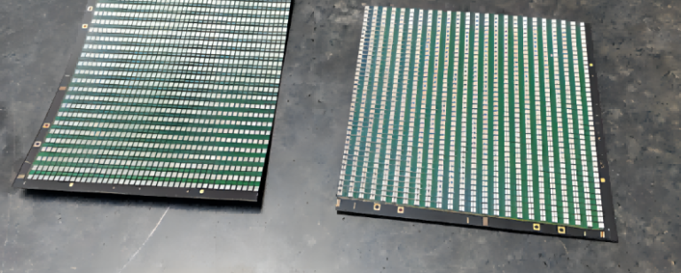
PCB Material Optimization Strategies
Selecting appropriate materials forms the foundation of high-quality PCB assembly (PCBA), directly influencing performance, thermal resilience, and longevity. Modern PCB assembly workflows prioritize substrates with optimal dielectric constants and thermal conductivity, such as FR-4, polyimide, or advanced ceramic-filled laminates, to minimize signal loss and withstand operational stressors. For high-frequency applications, low-loss materials like Rogers 4000 series are increasingly integrated to maintain signal integrity.
Another critical aspect involves surface finish selection. Options like Electroless Nickel Immersion Gold (ENIG) or Immersion Silver enhance solderability while preventing oxidation, ensuring robust connections in PCBA processes. Additionally, halogen-free laminates are gaining traction to meet environmental regulations without compromising flame retardancy.
Material optimization extends to solder mask choices, where liquid photoimageable (LPI) variants provide precise coverage, improving insulation and resistance to moisture or chemical exposure. Advanced thermal management strategies, such as incorporating metal-core substrates or thermally conductive adhesives, further mitigate heat-related failures in densely packed designs.
By aligning material properties with application-specific demands—whether for aerospace, automotive, or consumer electronics—manufacturers achieve reliable PCB assembly outcomes that balance cost, durability, and performance. This strategic approach ensures compatibility with automated assembly lines while meeting stringent quality benchmarks.
Boost PCB Performance and Durability
Achieving optimal performance and longevity in PCB assembly requires a strategic focus on material selection, design optimization, and environmental resilience. Modern PCBA processes prioritize the use of high-Tg laminates and low-loss dielectric substrates, which minimize signal distortion and enhance thermal stability under demanding operating conditions. By integrating advanced copper weights and trace geometries, engineers can reduce impedance mismatches, ensuring consistent signal integrity across high-frequency applications.
Thermal management remains a cornerstone of durable PCB assembly, with techniques like embedded heatsinks and thermal vias effectively dissipating heat from critical components. Pairing these with robust surface finishes, such as ENIG (Electroless Nickel Immersion Gold), prevents oxidation and improves solder joint reliability—key factors in extending product lifecycles. Additionally, conformal coatings and potting compounds shield assemblies from moisture, dust, and chemical exposure, further bolstering durability.
To maintain alignment with industry standards, rigorous testing protocols—including thermal cycling and vibration resistance assessments—validate the resilience of PCBA designs. By harmonizing material innovation with precision engineering, manufacturers can deliver electronics that excel in both performance and endurance, meeting the evolving demands of sectors like automotive, aerospace, and IoT.
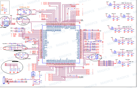
Innovative PCB Assembly Methods
Modern PCB assembly processes are evolving to address the growing complexity of electronic devices, with PCBA manufacturers adopting groundbreaking approaches to improve precision and scalability. One such advancement is additive manufacturing for circuit board fabrication, which enables the creation of multilayer designs with reduced material waste. Techniques like laser-assisted soldering are replacing traditional methods, offering micron-level accuracy for components as small as 01005 packages. Additionally, embedded component technology—where passive elements are integrated directly into substrate layers—minimizes footprint and enhances signal integrity in high-density applications.
Another transformative trend is the integration of flexible hybrid electronics (FHE) into PCB assembly workflows. By combining rigid and flexible substrates, FHE supports curved or wearable device architectures without compromising durability. Automated pick-and-place systems equipped with machine vision further refine PCBA quality, ensuring component alignment within ±25μm tolerances. These systems now leverage AI-driven algorithms to predict and correct placement errors in real time, reducing rework rates by up to 40%.
To maintain coherence with broader manufacturing goals, these innovations align with PCB material optimization strategies and thermal management solutions, forming a holistic approach to next-generation electronics production. As Industry 4.0 principles permeate PCB assembly facilities, IoT-enabled monitoring tools provide granular data analytics, enabling proactive adjustments to soldering profiles and material handling protocols. This synergy between cutting-edge techniques and data-driven oversight ensures consistent outcomes in high-performance PCBA applications.
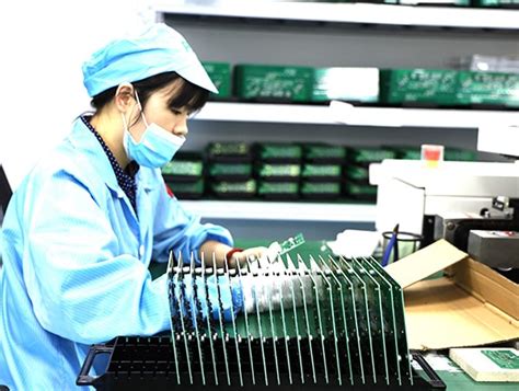
Quality Control in PCB Assembly
Effective quality control (QC) protocols form the backbone of dependable PCB assembly processes, ensuring each pcba meets stringent performance and reliability standards. Modern QC frameworks integrate automated optical inspection (AOI) systems to detect soldering defects, component misalignment, or trace irregularities at micron-level precision. These systems work in tandem with X-ray inspection for verifying hidden connections in multilayer boards or ball grid array (BGA) packages.
Material consistency is equally critical, with ionic contamination testing and thermal cycling validating the durability of solder joints and substrate integrity under stress. Advanced PCBA lines employ statistical process control (SPC) to monitor production trends, flagging deviations in real time to prevent batch failures. For mission-critical applications, environmental stress screening (ESS) simulates extreme operating conditions, exposing latent defects before deployment.
Transitioning seamlessly from automated inspection to final validation, QC protocols ensure alignment with design specifications while maintaining compliance with industry standards like IPC-A-610. By embedding these checks throughout the PCB assembly workflow, manufacturers minimize rework costs and deliver high-yield outcomes—key to sustaining competitiveness in precision electronics manufacturing.
Reliable PCB Soldering Techniques
Achieving consistent soldering quality is foundational to high-quality PCB assembly, as even minor defects can compromise electrical connectivity and long-term reliability. Modern PCBA processes leverage advanced techniques such as reflow soldering and wave soldering, which balance precision and scalability. For surface-mount components, reflow soldering employs controlled temperature profiles to melt solder paste uniformly, minimizing voids or cold joints. Through-hole components, meanwhile, often benefit from wave soldering, where boards pass over a molten solder wave to create robust connections.
To enhance reliability, manufacturers prioritize solder paste stencil design and thermal profiling. A well-engineered stencil ensures accurate solder deposition, while real-time thermal monitoring guarantees optimal reflow conditions. Additionally, selective soldering systems enable targeted heat application for mixed-technology boards, reducing thermal stress on sensitive components.
Material selection also plays a critical role. High-purity solder alloys with low oxidation rates improve joint integrity, especially in harsh environments. Pairing these with automated optical inspection (AOI) systems allows rapid detection of soldering anomalies, ensuring defects are addressed before final PCB assembly. By integrating these methodologies, manufacturers achieve repeatable results that meet stringent performance standards for modern electronics.
PCB Thermal Management Solutions
Effective thermal management is a cornerstone of high-quality PCB assembly, ensuring long-term reliability in electronic devices. As component densities increase and power requirements grow, managing heat dissipation becomes critical to prevent thermal stress, which can lead to premature failure. Advanced PCBA designs incorporate thermally conductive materials such as ceramic-filled substrates or metal-core boards, which redirect heat away from sensitive components.
A key strategy involves optimizing copper pour patterns and thermal vias to enhance heat distribution across the board. For high-power applications, integrating heat sinks or embedded cooling channels during PCB assembly ensures consistent temperature regulation. Additionally, selecting low-thermal-resistance solder alloys minimizes hotspots at junction points, preserving electrical integrity.
Automated inspection tools, like infrared thermography, are now integral to PCBA quality control, enabling real-time monitoring of thermal profiles during testing. This data-driven approach allows engineers to refine layouts and material choices, balancing performance with thermal efficiency.
Finally, environmental factors such as operating temperature ranges must align with the device’s application—whether industrial, automotive, or consumer electronics. By combining material science, design innovation, and precision manufacturing, high-quality PCB assembly achieves optimal thermal management, extending product lifespans while maintaining operational stability.
Conclusion
The pursuit of high-quality PCB assembly hinges on integrating advanced methodologies that balance precision, efficiency, and sustainability. As modern electronics demand greater reliability, manufacturers must prioritize process consistency and material integrity to ensure optimal performance. By leveraging automated optical inspection (AOI) systems and precision soldering technologies, PCBA workflows achieve tighter tolerances while minimizing human error. Equally critical is the adoption of thermal management solutions and high-performance substrates, which mitigate operational stressors and extend product lifespans.
To maintain competitiveness, the industry must continually refine PCB assembly protocols, incorporating data-driven quality control frameworks and eco-conscious material choices. Innovations like laser-assisted soldering and real-time analytics are redefining standards, enabling faster defect detection and corrective action. Ultimately, the success of PCBA projects relies on harmonizing cutting-edge techniques with rigorous testing regimes—ensuring each assembly meets the exacting demands of today’s dynamic electronic applications. This holistic approach not only elevates durability but also reinforces trust in the reliability of next-generation devices.

FAQs
What distinguishes high-quality PCB assembly from standard processes?
High-quality PCB assembly prioritizes precision in component placement, automated inspection for defect detection, and advanced thermal management to ensure long-term reliability. Unlike standard methods, it incorporates rigorous quality control protocols, such as X-ray testing for hidden solder joints.
How does material selection impact PCB performance?
Optimal material choices—like high-Tg substrates or low-loss laminates—directly influence signal integrity and thermal stability. In PCBA, pairing materials with the right solder masks and finishes reduces oxidation risks, enhancing durability in demanding environments.
Can automated systems improve assembly accuracy?
Yes. Automated optical inspection (AOI) and pick-and-place machines achieve micron-level precision, minimizing human error. These systems also enable real-time data analysis, allowing faster adjustments during PCB assembly workflows.
What role does soldering play in reliable PCBA?
Consistent soldering techniques, such as reflow or selective soldering, ensure strong electrical connections. For high-reliability PCBA, nitrogen-controlled environments prevent voids and cracks, critical for aerospace or medical devices.
Why is thermal management vital in modern PCB designs?
Advanced electronics generate significant heat, which degrades components over time. Techniques like embedded heat sinks or thermally conductive substrates in PCB assembly dissipate energy efficiently, extending product lifespans.
Ready to Optimize Your PCB Assembly Process?
For tailored solutions in high-quality PCB assembly, please click here to explore cutting-edge services that align with your project’s technical requirements.