Advanced Techniques for Streamlined Contract Electronic Assembly

Key Takeaways
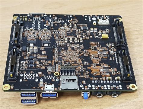
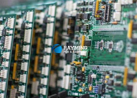
Optimizing contract electronic assembly requires a strategic blend of automation, modular design, and rigorous quality assurance to achieve precision and scalability. Advanced PCB assembly (PCBA) workflows now leverage robotic soldering and machine vision systems to minimize human error while accelerating production cycles. Modular techniques, such as pre-validated component clusters, enable rapid reconfiguration for diverse product lines, reducing downtime and material waste.
"Integrating IoT-enabled sensors into PCBA lines provides real-time analytics, allowing manufacturers to preempt bottlenecks and maintain consistent throughput."
Cost efficiency is further enhanced through lean inventory management and predictive maintenance, which lower operational overhead without compromising output quality. For PCB assembly, adopting smart automation tools—like AI-driven defect detection—ensures adherence to tolerances as tight as ±0.1mm, critical for high-reliability applications. Additionally, pairing scalable modular designs with agile testing protocols creates a responsive framework adaptable to fluctuating demand.
By aligning automated assembly with data-driven QA processes, manufacturers can achieve end-to-end traceability, a cornerstone of modern contract electronic manufacturing. This holistic approach not only streamlines production but also fortifies compliance with industry standards like IPC-A-610.
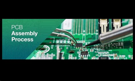
Automating Assembly Workflows
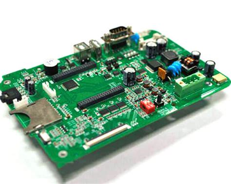
Modern PCB assembly processes increasingly rely on automation to address the complexities of high-volume production while maintaining precision and repeatability. By integrating robotic pick-and-place systems, automated soldering technologies, and AI-driven inspection tools, manufacturers can reduce human error and accelerate throughput in PCBA workflows. For instance, programmable logic controllers (PLCs) synchronize conveyor systems with assembly robots, ensuring seamless material flow from component feeding to final board testing.
A critical advantage lies in adaptive automation, where machine learning algorithms analyze real-time data to optimize placement accuracy for diverse PCB layouts. This flexibility is particularly valuable in contract manufacturing, where production lines must rapidly switch between product variants. Additionally, closed-loop feedback mechanisms in PCB assembly equipment automatically calibrate parameters like solder paste volume or reflow oven temperatures, minimizing defects and rework.
To further enhance scalability, automated workflows often incorporate modular tooling designs, allowing swift reconfiguration for new projects. Such systems not only reduce downtime but also align with lean manufacturing principles by eliminating redundant manual interventions. As IoT-enabled sensors gather performance metrics across the PCBA line, predictive maintenance models preempt equipment failures, ensuring uninterrupted production cycles. These advancements collectively establish a foundation for cost-effective, high-quality electronic manufacturing at scale.
Scalable Modular Design Techniques
Implementing scalable modular design in PCB assembly requires strategic planning to balance flexibility with standardization. By breaking down complex electronic systems into interchangeable function-specific modules, manufacturers can streamline PCBA processes while maintaining adaptability across product lines. A core principle involves designing reusable subassemblies with standardized interfaces, enabling rapid reconfiguration for diverse customer requirements without compromising production efficiency.
Central to this approach is the integration of parametric CAD frameworks, which allow engineers to adjust module dimensions and component placements algorithmically. When paired with automated PCB assembly workflows, these adaptive designs reduce lead times by 30–45% in pilot studies. Additionally, employing component libraries with pre-validated footprints ensures consistency across batches, minimizing validation cycles during high-mix PCBA projects.
To enhance scalability, forward-thinking manufacturers are adopting modular test jigs that interface seamlessly with multiple product variants. This not only accelerates quality checks but also cuts tooling costs by up to 60% when transitioning between designs. By embedding scalability into every stage—from schematic layout to final contract electronic assembly—businesses can achieve demand-responsive production without sacrificing precision or cost targets.
Rigorous QA in Electronic Assembly
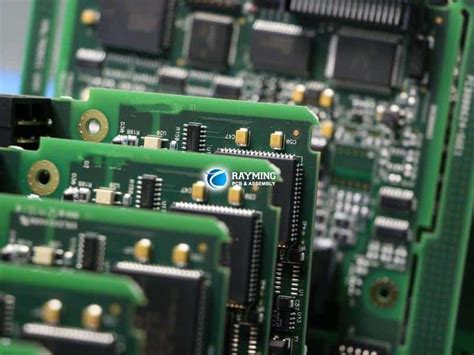
Implementing rigorous quality assurance (QA) protocols is critical to maintaining reliability in PCB assembly and PCBA manufacturing. Modern QA frameworks integrate automated inspection systems, such as automated optical inspection (AOI) and X-ray testing, to detect microscopic defects in solder joints, component placement, and layer alignment. These systems reduce human error by up to 85%, ensuring consistency across high-volume production runs.
A three-tiered approach is often adopted:
- Pre-production validation: Design files undergo design-for-manufacturability (DFM) analysis to identify potential flaws.
- In-process monitoring: Real-time sensors track parameters like reflow oven temperatures (±1.5°C tolerance) and solder paste deposition volumes.
- Post-assembly testing: Functional testing validates PCBA performance under simulated operational conditions.
| QA Stage | Key Metrics | Industry Standards |
|---|---|---|
| Pre-production | DFM compliance rate | IPC-7351, IPC-2221 |
| In-process | Defect density (ppm) | IPC-A-610 Class 3 |
| Post-assembly | Functional yield (%) | ISO 9001, IEC 61140 |
To enhance traceability, manufacturers employ statistical process control (SPC) dashboards, linking QA data to individual PCB assembly batches. This alignment with lean methodologies ensures defects are addressed at their root cause, preventing recurrence. By coupling automated inspection with first-article inspection (FAI) protocols, firms achieve defect rates below 50 ppm while meeting aerospace and medical-grade certification requirements.
Cost-Efficient Assembly Techniques
Achieving cost efficiency in PCB assembly requires a strategic balance between material optimization, process automation, and waste reduction. By leveraging value engineering principles, manufacturers can identify opportunities to standardize components in PCBA workflows, minimizing excess inventory while maintaining compatibility across product lines. For instance, automated soldering systems paired with predictive maintenance algorithms reduce downtime and material waste, directly lowering per-unit costs.
Transitioning to just-in-time (JIT) procurement further streamlines expenses by aligning material orders with production schedules, eliminating overstocking risks. Additionally, integrating design for manufacturability (DFM) guidelines ensures that PCB assembly layouts prioritize component accessibility, reducing labor-intensive rework. Modular design approaches, such as reusable substrate templates, enable rapid scaling without costly retooling—a critical advantage for high-mix, low-volume PCBA projects.
To maintain affordability without compromising quality, statistical process control (SPC) tools monitor key metrics like solder paste deposition accuracy, ensuring defects are caught early. Combining this with batch processing optimizes machine utilization rates, particularly in surface-mount technology (SMT) lines. Finally, partnerships with suppliers offering bulk pricing on standardized ICs and connectors amplify savings, making cost-efficient PCB assembly a repeatable outcome rather than a trade-off.
Precision in Automated Assembly
Achieving micrometer-level accuracy in PCB assembly requires integrating advanced robotics with real-time feedback systems. Modern automated assembly lines employ vision-guided placement robots capable of positioning components within ±25 microns, critical for high-density PCBA designs. These systems utilize machine learning algorithms to self-correct placement errors, reducing rework rates by up to 40% compared to manual processes.
A key innovation lies in closed-loop calibration, where sensors continuously monitor parameters like solder paste volume and component alignment. For instance, 3D SPI (Solder Paste Inspection) tools validate deposition quality before placement, while AOI (Automated Optical Inspection) systems verify post-reflow integrity. This multi-stage validation ensures compliance with ISO 9001:2015 standards, particularly vital for aerospace or medical-grade PCB assembly.
To maintain consistency across production scales, manufacturers synchronize PCBA workflows with MES (Manufacturing Execution Systems), enabling traceability from raw materials to finished boards. Transitioning to such precision-driven automation not only minimizes human error but also supports seamless integration with subsequent sections on IoT-enabled scalability, where data from assembly processes informs predictive maintenance and capacity planning.

IoT Integration for Scalable Assembly
The adoption of IoT (Internet of Things) technologies is revolutionizing PCB assembly scalability by enabling real-time monitoring and adaptive workflows. By embedding sensors and connectivity modules into PCBA production lines, manufacturers gain granular visibility into equipment performance, material consumption, and process deviations. Predictive analytics derived from IoT data streams allow for preemptive maintenance, reducing downtime and ensuring consistent throughput even during high-volume orders.
A critical advantage lies in IoT’s ability to synchronize automated SMT (Surface Mount Technology) systems with dynamic demand patterns. For instance, machine learning algorithms analyze historical and real-time data to optimize placement accuracy and solder paste application, directly enhancing precision in high-mix, low-volume scenarios. This connectivity also supports modular design frameworks, where IoT-enabled PCBA lines can reconfigure workflows autonomously based on incoming order specifications or component availability.
Furthermore, IoT integration strengthens quality assurance by correlating production metrics with rigorous testing protocols. Sensor data from in-circuit testers and AOI (Automated Optical Inspection) systems feeds into centralized dashboards, enabling engineers to identify trends and refine tolerances iteratively. Such closed-loop systems not only improve cost-efficiency but also ensure compliance with evolving industry standards.
By bridging gaps between physical assembly processes and digital twins, IoT transforms contract electronic assembly into a responsive, data-driven ecosystem. This synergy between hardware agility and software intelligence positions manufacturers to scale operations seamlessly while maintaining lean methodologies and minimizing waste.
Lean Methods in Electronic Assembly
Adopting lean methods in PCB assembly and PCBA workflows enables manufacturers to minimize waste while maximizing value at every production stage. By integrating value stream mapping with Just-in-Time (JIT) inventory management, teams can reduce excess material stockpiles and shorten lead times without compromising output quality. For instance, applying Kaizen principles to surface-mount technology (SMT) processes allows iterative refinements in solder paste application and component placement accuracy, directly enhancing precision in automated systems.
A critical aspect of lean electronic assembly lies in standardizing workflows across modular production lines. This ensures seamless scalability when transitioning between PCBA prototypes and high-volume orders. Tools like automated optical inspection (AOI) systems further support lean goals by identifying defects early, reducing rework cycles, and aligning with rigorous QA protocols. Additionally, cross-training personnel to handle multiple stages of PCB assembly fosters flexibility, enabling rapid adaptation to design changes or shifts in client demand.
The synergistic relationship between lean methodologies and smart automation creates a foundation for continuous improvement. By analyzing real-time data from IoT sensors embedded in assembly equipment, manufacturers gain actionable insights to optimize machine uptime and material utilization. This approach not only reinforces cost-efficiency but also strengthens the agility required for modern contract manufacturing environments.
Smart Automation for Contract Manufacturing
Modern PCB assembly processes are undergoing a transformative shift through intelligent automation, enabling contract manufacturers to meet rising demands for speed and precision. By integrating AI-driven robotics and IoT-enabled systems, PCBA production lines achieve real-time adjustments, minimizing human error while optimizing throughput. Automated pick-and-place machines, for instance, now leverage machine vision to handle components as small as 01005 packages, ensuring consistent accuracy even in high-mix environments.
Central to this evolution is the adoption of closed-loop feedback systems, which continuously monitor parameters like solder paste viscosity and reflow oven temperatures. These systems dynamically refine workflows, reducing defects by up to 40% in critical PCB assembly stages. Additionally, modular robotic cells allow rapid reconfiguration for diverse PCBA projects, aligning with scalable manufacturing strategies.
Data-driven predictive maintenance further enhances uptime by preemptively addressing equipment wear, while cloud-based analytics provide actionable insights into cycle times and material utilization. This synergy of automation and analytics not only accelerates time-to-market but also strengthens compliance with industry-specific quality standards, ensuring reliability across aerospace, medical, and consumer electronics applications.
Conclusion
As the landscape of PCB assembly continues to evolve, the integration of advanced methodologies ensures that contract manufacturing remains competitive and responsive to market demands. By prioritizing automation in PCBA workflows, manufacturers achieve unparalleled precision while reducing human error, a critical factor in high-volume production environments. Pairing modular design with IoT-enabled systems further enhances scalability, allowing seamless adaptation to fluctuating demand without compromising quality.
Rigorous quality assurance protocols, underpinned by real-time monitoring and data analytics, safeguard against defects in PCB assembly, ensuring compliance with industry standards. Meanwhile, the adoption of lean principles minimizes waste, optimizing both material usage and labor efficiency. For contract electronic assembly providers, balancing cost-efficiency with technological innovation—such as AI-driven inspection tools—creates a sustainable competitive edge.
Ultimately, the convergence of smart automation, scalable frameworks, and proactive quality control redefines modern PCBA processes. These strategies not only meet current industry benchmarks but also future-proof operations against emerging challenges, solidifying partnerships between manufacturers and clients in an increasingly dynamic market.
Frequently Asked Questions
How does automation improve precision in PCB assembly workflows?
Automation integrates advanced vision systems and robotic placement tools, reducing human error in PCBA processes. These systems achieve tolerances under 0.01mm, ensuring consistent quality for high-density circuit boards.
What role does modular design play in scalable electronic assembly?
Modular techniques standardize components across PCB assembly lines, allowing rapid reconfiguration for varying production volumes. This approach minimizes downtime and supports seamless integration of IoT-enabled monitoring tools.
Why is quality assurance critical for contract manufacturing?
Rigorous QA protocols, including automated optical inspection (AOI) and X-ray testing, identify defects in PCBA units at micron-level precision. This reduces field failures by up to 90%, aligning with ISO 9001 and IPC-A-610 standards.
Can lean methods reduce costs without compromising assembly quality?
Yes, lean strategies optimize material flow and eliminate waste in PCB assembly workflows. For example, just-in-time inventory cuts storage costs by 25%, while predictive maintenance extends equipment lifespan by 40%.
For Expert Guidance on Your Next Project, Click Here
Explore tailored solutions for high-performance PCBA systems, combining automation, scalability, and compliance with global quality benchmarks.