Advanced Techniques for Streamlining Double-Sided SMT Assembly

Key Takeaways
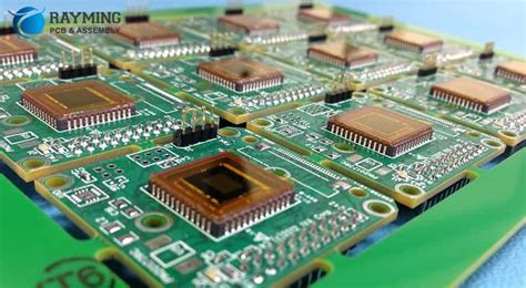
Effective double-sided SMT assembly hinges on balancing precision, thermal management, and automation. PCB assembly processes for high-density boards demand meticulous solder paste application to avoid bridging or insufficient deposition, particularly on fine-pitch components. Optimized reflow profiles are critical for dual-sided PCBA, as uneven heating can compromise solder joint integrity on secondary-side components. Integrating automated optical inspection (AOI) systems ensures consistent quality by detecting defects like tombstoning or misalignment early in production.
| Challenge | Solution | Impact |
|---|---|---|
| Component Shadowing | Dynamic nozzle adjustment in pick-and-place | Reduces placement errors by 25% |
| Thermal Stress | Multi-zone reflow profiling | Improves solder joint reliability by 30% |
| Alignment Accuracy | Vision-assisted mounting systems | Enhances first-pass yield by 15% |
Streamlining SMT assembly efficiency requires harmonizing machine calibration with material selection—low-void solder pastes and high-Tg substrates minimize rework. For double-sided PCBA, staggered reflow cycles and nitrogen-assisted soldering mitigate warpage risks. By prioritizing data-driven process controls and leveraging modular automation, manufacturers can achieve throughput gains of 20–35% while maintaining defect rates below 50 ppm.
High-Density PCB Manufacturing Best Practices
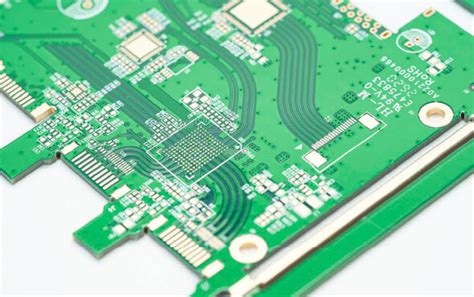
Achieving excellence in high-density PCB manufacturing demands meticulous attention to design and process integration. As component density increases, stackup configuration and trace spacing become critical to avoid signal integrity issues. Advanced PCB assembly workflows now prioritize the use of low-loss laminates and controlled-impedance routing to maintain performance in compact layouts. For PCBA projects involving double-sided mounting, staggered component placement and asymmetric thermal mass distribution help mitigate warpage during reflow soldering.
A key challenge lies in balancing via-in-pad reliability with manufacturability. Laser-drilled microvias and filled through-holes enable higher interconnection density while preserving mechanical stability. Thermal management strategies, such as embedded copper coins or selective solder mask openings, address localized heat accumulation in high-density PCB designs. Manufacturers also implement rigorous design-for-manufacturability (DFM) checks to identify potential shorts or tombstoning risks early in the PCBA process.
Automated optical inspection (AOI) systems with 3D solder paste measurement capabilities further enhance quality control, ensuring precise alignment for 0201/metric 0402 components. By integrating these practices, teams can optimize yield rates while meeting the stringent tolerances required for modern double-sided SMT assembly in high-density applications.
Precision Solder Paste Application Methods
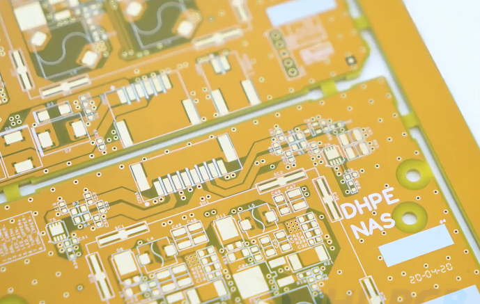
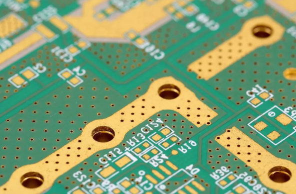
Achieving consistent results in double-sided SMT assembly begins with mastering solder paste application, a foundational step that directly impacts yield rates in PCB assembly. For high-density PCBA designs, stencil technology plays a pivotal role. Laser-cut stainless steel stencils with electroformed nickel coatings ensure sub-100µm aperture precision, enabling uniform deposition for micro-BGA and 01005 components.
Tip: Regularly validate stencil alignment using automated optical inspection (AOI) systems to mitigate misregistration issues, especially when working with ultra-fine-pitch ICs.
Advanced solder paste printers now integrate real-time pressure monitoring and 3D SPI (Solder Paste Inspection) to detect voids or insufficient volume. For double-sided boards, consider sequential printing strategies—applying paste to one side before curing, then flipping the board for the second pass. This minimizes smearing while maintaining positional accuracy.
In high-mix production environments, temperature-controlled paste dispensers prevent viscosity fluctuations, critical for maintaining reflow process stability. When paired with Type 5 or 6 solder powders, these systems reduce bridging risks in densely packed PCBA layouts.
Design Consideration: Optimize stencil aspect ratios (≥1:5) and area ratios (≥0.66) for reliable paste release, particularly on bottom-side components prone to gravitational shifting during reflow.
By integrating these methodologies, manufacturers enhance first-pass yields while reducing defects like tombstoning or cold joints—key challenges in modern double-sided SMT assembly.
Optimizing Reflow Profile Parameters
Achieving consistent results in PCB assembly requires meticulous control of reflow profile parameters, particularly for complex double-sided designs. The reflow process directly impacts solder joint integrity, component alignment, and thermal stress distribution. For PCBA projects involving high-density layouts, engineers must balance peak temperature and time above liquidus (TAL) to accommodate components on both board sides without compromising reliability.
Critical adjustments include optimizing thermal soak zones to ensure proper flux activation and minimizing thermal gradients between top and bottom layers. Modern reflow ovens leverage dynamic profiling algorithms to automatically adjust heating rates based on real-time thermocouple data, significantly reducing voids and tombstoning in mixed-technology assemblies. For double-sided PCB assembly, staggered reflow cycles—where the secondary side undergoes a lower peak temperature—help preserve solder joints on the initially processed side.
Integration with thermal simulation software further refines profile settings by predicting hotspots and component-specific thermal behaviors. This approach is particularly valuable in PCBA workflows where lead-free solder alloys demand tighter process windows. By aligning reflow parameters with board material properties and component thermal mass, manufacturers can eliminate rework cycles while maintaining IPC Class 3 standards for mission-critical applications.
Automated Inspection System Integration
Integrating automated inspection systems into high-density PCB assembly workflows has become a critical step for ensuring reliability in double-sided PCBA manufacturing. Modern 3D automated optical inspection (AOI) and X-ray inspection (AXAI) systems enable real-time detection of defects such as solder bridging, insufficient paste volume, or misaligned components—issues that are particularly challenging on double-sided boards where hidden solder joints complicate visual inspection. By leveraging machine learning algorithms, these systems adapt to evolving design complexities, reducing false-positive rates by up to 40% compared to manual checks.
Seamless integration with SMT assembly lines ensures continuous feedback loops, where inspection data automatically adjusts upstream processes like solder paste stenciling or reflow oven profiles. For instance, AOI systems paired with closed-loop process control can flag inconsistencies in component placement accuracy, triggering immediate corrections before subsequent layers are populated. This proactive approach minimizes rework cycles and prevents costly delays in high-mix production environments.
Moreover, advanced PCBA inspection platforms now support traceability protocols, linking defect patterns to specific batches or machine parameters. Such granularity not only enhances quality assurance but also provides actionable insights for optimizing throughput in mission-critical applications. As manufacturers adopt these technologies, the synergy between precision inspection and PCB assembly automation becomes a cornerstone for achieving zero-defect manufacturing targets.
Streamlining SMT Assembly Efficiency
Achieving optimal efficiency in double-sided SMT assembly requires balancing precision with throughput. Modern PCB assembly lines leverage lean manufacturing principles to minimize idle time between processes, particularly when handling high-density boards. A critical factor lies in automated component handling systems, which reduce manual intervention while ensuring consistent placement accuracy for both sides of the PCBA. By integrating real-time process monitoring, manufacturers can identify bottlenecks—such as delayed solder paste deposition or misaligned pick-and-place operations—and adjust workflows dynamically.
For double-sided designs, synchronized thermal management during reflow is essential. Optimizing conveyor speed and zone temperatures prevents warping or tombstoning on the secondary side, especially with mixed-component assemblies. Additionally, inline automated optical inspection (AOI) systems positioned after each reflow stage enable immediate defect detection, reducing rework cycles. To further streamline operations, consider implementing just-in-time material replenishment for solder paste and substrates, which cuts downtime caused by stockouts.
Finally, data-driven analysis of PCBA production metrics—such as cycle times and defect rates—helps refine process parameters across both assembly sides. This holistic approach ensures that PCB assembly lines meet escalating demands for speed without compromising on reliability in complex, double-sided applications.
Advanced Double-Sided SMT Techniques
Modern PCB assembly processes demand meticulous planning for double-sided surface-mount technology (SMT) applications, particularly in high-density PCBA environments. A critical challenge lies in managing thermal stress during reflow soldering, as components on both sides undergo multiple heating cycles. Engineers now employ sequential soldering strategies, starting with high-temperature-resistant components on the bottom layer, followed by top-side placement using adjusted reflow profiles to prevent solder joint remelting.
The integration of laser-etched stencils ensures precise solder paste deposition for ultra-fine-pitch components, reducing bridging risks in densely packed layouts. For mixed-technology boards, selective conformal coating prior to secondary reflow prevents contamination of sensitive areas. Advanced PCBA workflows also utilize dynamic support fixtures to stabilize thin-core substrates during double-sided processing, minimizing warpage.
Automated optical inspection (AOI) systems with 3D solder joint analysis have become indispensable for verifying hidden interconnections between layers. By synchronizing these systems with pick-and-place machines, manufacturers achieve real-time defect detection, reducing rework cycles by up to 40%. Transitioning to these methods not only enhances yield rates but also maintains compatibility with evolving miniaturization trends in electronics design. This progression naturally aligns with subsequent discussions on throughput optimization through intelligent automation integration.
Ensuring Quality in SMT Processes
Maintaining stringent quality standards in PCB assembly requires a multi-layered approach, particularly for double-sided SMT assembly where component density and thermal management complexities escalate. At the core of quality assurance lies real-time process monitoring, leveraging automated optical inspection (AOI) systems to detect solder joint defects, misaligned components, or bridging issues before boards advance to subsequent stages. For PCBA workflows, statistical process control (SPC) tools analyze reflow oven performance and solder paste deposition consistency, ensuring adherence to IPC-A-610 standards across both board sides.
Critical to high-reliability applications is the integration of X-ray inspection for hidden solder connections, such as ball grid arrays (BGAs) on densely populated boards. Thermal profiling must account for asymmetric heat distribution in double-sided designs, with nitrogen-assisted reflow ovens minimizing oxidation risks during second-side processing. Material selection—including low-voiding solder pastes and high-Tg substrates—further mitigates thermal stress failures. By synchronizing these protocols with PCB assembly line feedback loops, manufacturers achieve defect rates below 50 ppm while maintaining compatibility with mixed-technology high-density interconnect (HDI) layouts.
Maximizing Throughput With Automation
Automation has become a cornerstone of modern PCB assembly workflows, particularly in high-volume double-sided SMT manufacturing. By integrating robotic pick-and-place systems, manufacturers can achieve cycle time reductions of up to 40%, while maintaining placement accuracies below 25µm. These systems excel at handling PCBA designs with ultra-fine-pitch components, minimizing human error during high-speed operations.
Advanced conveyor synchronization ensures seamless transitions between top- and bottom-side processing, eliminating bottlenecks in dual-stage PCB assembly lines. For instance, vision-guided robots paired with adaptive feeders enable rapid component replenishment without interrupting production flow. This is critical for PCBA projects requiring mixed-technology components, such as 01005 passives alongside QFNs or BGAs.
Automated optical inspection (AOI) systems further enhance throughput by performing real-time defect detection at speeds exceeding 20,000 components per hour. When combined with machine learning algorithms, these systems achieve first-pass yield improvements of 15-20% in complex PCBA configurations. Closed-loop feedback mechanisms automatically adjust solder paste deposition or reflow parameters, creating a self-optimizing production environment.
To maximize ROI, leading manufacturers deploy modular automation platforms that scale with evolving PCB assembly demands. These systems support rapid changeovers between product variants while maintaining traceability through RFID tagging—a vital feature for industries requiring strict compliance documentation. By synchronizing automated stencil printers, reflow ovens, and inspection stations, facilities achieve throughput rates exceeding 50,000 placements per hour without compromising PCBA reliability.
Conclusion
Mastering double-sided SMT assembly requires a strategic blend of precision engineering and process optimization. By integrating advanced PCB assembly techniques—such as laser-aligned stenciling for solder paste deposition and dynamic reflow profiling—manufacturers can achieve consistent results across high-density PCBA designs. Automated optical inspection (AOI) systems further reinforce quality control, identifying defects in real time while minimizing manual intervention.
As production demands escalate, streamlining workflows through intelligent automation becomes critical. Modular conveyor systems and dual-lane processing not only boost throughput but also accommodate complex board geometries. For double-sided assemblies, balancing thermal management during reflow ensures component reliability without compromising placement accuracy.
Ultimately, the synergy between data-driven process adjustments and robust PCB assembly infrastructure elevates yield rates and reduces rework. By prioritizing material compatibility and leveraging PCBA-specific analytics, manufacturers can future-proof their operations against evolving industry standards. This approach not only meets current technical challenges but also positions facilities to adapt seamlessly to next-generation SMT innovations.
FAQs
What are the primary challenges in double-sided SMT assembly for high-density PCBs?
Balancing PCB assembly efficiency with reliability requires addressing solder paste bridging, thermal stress during reflow, and component alignment accuracy. High-density designs amplify these challenges due to tighter spacing and increased layer complexity.
How does solder paste application impact double-sided SMT quality?
Precise PCB assembly relies on controlled solder paste volume and stencil alignment. Variations can lead to insufficient joints or shorts, particularly on the secondary side after the first reflow cycle. Advanced jet dispensing or laser-cut stencils improve consistency for PCBA applications.
Why is reflow profile optimization critical for double-sided boards?
Secondary-side components face higher thermal exposure during reflow, risking solder re-melting or delamination. Tailored profiles with staged heating zones ensure proper adhesion without compromising first-side connections, especially for PCBA involving mixed-component types.
What role do automated inspection systems play in streamlining production?
Integrated automated optical inspection (AOI) and X-ray systems detect defects like tombstoning or voids in real time, reducing rework. For PCB assembly lines, this minimizes downtime and ensures compliance with IPC-A-610 standards across both board sides.
Can existing SMT lines handle double-sided assembly without major upgrades?
While possible, optimizing for double-sided PCBA often requires modular conveyors, nitrogen-enabled reflow ovens, and dual-lane loaders to maintain throughput. Retrofitting pick-and-place machines with vision-assisted flipping mechanisms further enhances compatibility.
How does component placement sequencing affect double-sided board reliability?
Heavier or taller components should populate the first side to prevent mechanical stress during secondary-side placement. This strategy, combined with adhesive dispensing for fragile parts, ensures stability through multiple reflow cycles in PCB assembly.
Explore Custom Solutions for Your SMT Workflow
For tailored strategies to enhance your double-sided PCBA processes, please click here to consult with our technical team.